-
LM5102、高電圧ハーフブリッジ・ゲート・ドライバ、プログラマブル遅延付き
パッケージ・オプション
メカニカル・データ(パッケージ|ピン)
サーマルパッド・メカニカル・データ
発注情報
LM5102、高電圧ハーフブリッジ・ゲート・ドライバ、プログラマブル遅延付き
1 特長
- ハイサイドとローサイド両方のNチャネルMOSFETを駆動
- ハイサイドとローサイドの立ち上がりエッジ遅延時間を独立してプログラミング可能
- ブートストラップ電源電圧範囲:最大118V DC
- 高速ターンオフ伝搬遅延(標準25ns)
- 15nsの立ち上がり/立ち下がり時間で1000pFの負荷を駆動
- 電源レールの低電圧誤動作防止
- 低消費電力
- シーケンスの途中でタイマを終了可能
2 アプリケーション
- 電流供給プッシュプル・パワー・コンバータ
- ハーフ/フルブリッジのパワー・コンバータ
- 同期降圧コンバータ
- 2スイッチのフォワード・パワー・コンバータ
- アクティブ・クランプ型フォワード・コンバータ
3 概要
LM5102は、同期降圧型またはハーフブリッジの構成においてハイサイドとローサイド両方のNチャネルMOSFETを駆動するよう設計された、高電圧ゲート・ドライバです。フローティング・ハイサイド・ドライバは、最大100Vの電源電圧で動作できます。各出力は、それぞれ独立に制御されます。プログラミング抵抗を使用して、各出力の立ち上がりエッジを独立して遅延させることができます。ハイサイド・ゲート・ドライバのブートストラップ・コンデンサの充電用に高電圧ダイオードを内蔵しています。堅牢なレベル・シフタにより、消費電力を抑えながら高速で動作し、制御ロジックからハイサイド・ゲート・ドライバへのクリーンなレベル遷移を実現します。ローサイドとハイサイド両方の電源レールに低電圧誤動作防止機能が搭載されています。デバイスは標準のVSSOP 10ピンおよびWSON 10ピン・パッケージで供給されます。
製品情報(1)
| 型番 | パッケージ | 本体サイズ(公称) |
|---|---|---|
| LM5102 | VSSOP (10) | 3.00mm×3.00mm |
| WSON (10) | 4.00mm×4.00mm |
- 提供されているすべてのパッケージについては、巻末の注文情報を参照してください。
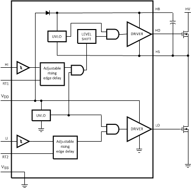
ブロック概略図
5 Pin Configuration and Functions

Pin Functions
| PIN | TYPE(2) | DESCRIPTION | APPLICATION INFORMATION | |
|---|---|---|---|---|
| NAME | WSON(1), VSSOP |
|||
| HB | 2 | P | High-side gate driver bootstrap rail | Connect the positive terminal of bootstrap capacitor to the HB pin and connect negative terminal of bootstrap capacitor to HS. The Bootstrap capacitor should be placed as close to IC as possible. |
| HI | 7 | I | High-side driver control input | TTL compatible thresholds. Unused inputs should be tied to ground and not left open. |
| HO | 3 | O | High-side gate driver output | Connect to gate of high-side MOSFET with short low-inductance path. |
| HS | 4 | P | High-side MOSFET source connection | Connect bootstrap capacitor negative terminal and source of high side MOSFET. |
| LI | 8 | I | Low-side driver control input | TTL compatible thresholds. Unused inputs should be tied to ground and not left open. |
| LO | 10 | O | Low-side gate driver output | Connect to the gate of the low side MOSFET with a short low inductance path. |
| RT1 | 5 | A | High-side output edge delay programming | Resistor from RT1 to ground programs the leading edge delay of the high side gate driver. The resistor should be placed close to the IC to minimize noise coupling from adjacent traces. |
| RT2 | 6 | A | Low-side output edge delay programming | Resistor from RT2 to ground programs the leading edge delay of the low side gate driver. The resistor should be placed close to the IC to minimize noise coupling from adjacent traces. |
| VDD | 1 | P | Positive gate drive supply | Locally decouple to VSS using low ESR/ESL capacitor, located as close to IC as possible. |
| VSS | 9 | G | Ground return | All signals are referenced to this ground. |
6 Specifications
6.1 Absolute Maximum Ratings(1)(2)
| MIN | MAX | UNIT | |
|---|---|---|---|
| VDD to VSS | –0.3 | 18 | V |
| VHB to VHS | –0.3 | 18 | V |
| LI or HI Inputs to VSS | –0.3 | VDD + 0.3 | V |
| LO Output | –0.3 | VDD + 0.3 | V |
| HO Output | VHS – 0.3 | VHB + 0.3 | V |
| VHS to VSS | –1 | 100 | V |
| VHB to VSS | 118 | V | |
| RT1 and RT2 to VSS | –0.3 | 5 | V |
| Junction Temperature | 150 | °C | |
| Storage Temperature Range | –55 | 150 | °C |
6.2 ESD Ratings
| VALUE | UNIT | |||
|---|---|---|---|---|
| V(ESD) | Electrostatic discharge | Human-body model (HBM), per ANSI/ESDA/JEDEC JS-001(1) | ±2000 | V |
6.3 Recommended Operating Conditions
| MIN | MAX | UNIT | |
|---|---|---|---|
| VDD | 9 | 14 | V |
| HS | –1 | 100 | V |
| HB | VHS + 8 | VHS + 14 | V |
| HS Slew Rate | < 50 | V/ns | |
| Junction Temperature | –40 | 125 | °C |
6.4 Thermal Information
| THERMAL METRIC(1) | LM5102 | UNIT | ||
|---|---|---|---|---|
| DGS | DPR(2) | |||
| 10 PINS | 10 PINS | |||
| RθJA | Junction-to-ambient thermal resistance | 165.3 | 37.9 | °C/W |
| RθJC(top) | Junction-to-case (top) thermal resistance | 58.9 | 38.1 | |
| RθJB | Junction-to-board thermal resistance | 54.4 | 14.9 | |
| ψJT | Junction-to-top characterization parameter | 6.2 | 0.4 | |
| ψJB | Junction-to-board characterization parameter | 83.6 | 15.2 | |
| RθJC(bot) | Junction-to-case (bottom) thermal resistance | N/A | 4.4 | |
6.5 Electrical Characteristics
Specifications in standard typeface are for TJ = +25°C. Unless otherwise specified, VDD = VHB = 12 V, VSS = VHS = 0V, RT1 = RT2 = 100 kΩ. No load on LO or HO.| PARAMETER | TEST CONDITIONS | MIN(1) | TYP | MAX(1) | UNIT | |
|---|---|---|---|---|---|---|
| SUPPLY CURRENTS | ||||||
| IDD | VDD Quiescent Current | LI = HI = 0 V | 0.4 | mA | ||
| LI = HI = 0 V, –40°C to +125°C | 0.6 | |||||
| IDDO | VDD Operating Current | f = 500 kHz | 1.5 | mA | ||
| f = 500 kHz, –40°C to +125°C | 3 | |||||
| IHB | Total HB Quiescent Current | LI = HI = 0 V | 0.06 | mA | ||
| LI = HI = 0 V, –40°C to +125°C | 0.2 | |||||
| IHBO | Total HB Operating Current | f = 500 kHz | 1.3 | mA | ||
| f = 500 kHz, –40°C to +125°C | 3 | |||||
| IHBS | HB to VSS Current, Quiescent | VHS = VHB = 100 V | 0.05 | µA | ||
| VHS = VHB = 100 V, –40°C to +125°C | 10 | |||||
| IHBSO | HB to VSS Current, Operating | f = 500 kHz | 0.08 | mA | ||
| INPUT PINS | ||||||
| VIL | Low Level Input Voltage Threshold | 1.8 | V | |||
| –40°C to +125°C | 0.8 | |||||
| VIH | High Level Input Voltage Threshold | 1.8 | V | |||
| –40°C to +125°C | 2.2 | |||||
| RI | Input Pulldown Resistance | 200 | kΩ | |||
| –40°C to +125°C | 100 | 500 | ||||
| TIME DELAY CONTROLS | ||||||
| VRT | Nominal Voltage at RT1, RT2 | 3 | V | |||
| –40°C to +125°C | 2.7 | 3.3 | ||||
| IRT | RT Pin Current Limit | RT1 = RT2 = 0 V | 1.5 | mA | ||
| RT1 = RT2 = 0 V, –40°C to +125°C | 0.75 | 2.25 | ||||
| Vth | Timer Termination Threshold | 1.8 | V | |||
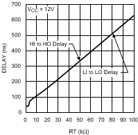
| TDL1, TDH1 | Rising edge turn-on delay, RT = 10 kΩ | 105 | ns | |||
| –40°C to +125°C | 75 | 150 | ||||
| TDL2, TDH2 | Rising edge turn-on delay, RT = 100 kΩ | 630 | ns | |||
| –40°C to +125°C | 530 | 750 | ||||
| UNDER VOLTAGE PROTECTION | ||||||
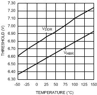
| VDDR | VDD Rising Threshold | 6.9 | V | |||
| –40°C to +125°C | 6.0 | 7.4 | ||||
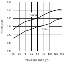
| VDDH | VDD Threshold Hysteresis | 0.5 | V | |||
| VHBR | HB Rising Threshold | 6.6 | V | |||
| –40°C to +125°C | 5.7 | 7.1 | ||||
| VHBH | HB Threshold Hysteresis | 0.4 | V | |||
| BOOTSTRAP DIODE | ||||||
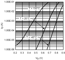
| VDL | Low-Current Forward Voltage | IVDD-HB = 100 µA | 0.60 | V | ||
| IVDD-HB = 100 µA, –40°C to +125°C | 0.9 | |||||
| VDH | High-Current Forward Voltage | IVDD-HB = 100 mA | 0.85 | V | ||
| IVDD-HB = 100 mA, –40°C to +125°C | 1.1 | |||||
| RD | Dynamic Resistance | IVDD-HB = 100 mA | 0.8 | Ω | ||
| IVDD-HB = 100 mA, –40°C to +125°C | 1.5 | |||||
| LO GATE DRIVER | ||||||
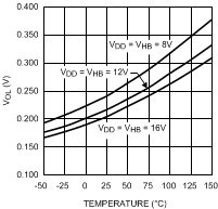
| VOLL | Low-Level Output Voltage | ILO = 100 mA | 0.25 | V | ||
| ILO = 100 mA, –40°C to +125°C | 0.4 | |||||
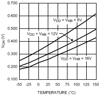
| VOHL | High-Level Output Voltage | ILO = –100 mA, VOHL = VDD – VLO | 0.35 | V | ||
| ILO = –100 mA, VOHL = VDD – VLO, –40°C to +125°C | 0.55 | |||||
| IOHL | Peak Pullup Current | VLO = 0 V | 1.6 | A | ||
| IOLL | Peak Pulldown Current | VLO = 12 V | 1.8 | A | ||
| HO GATE DRIVER | ||||||
| VOLH | Low-Level Output Voltage | IHO = 100 mA | 0.25 | V | ||
| IHO = 100 mA, –40°C to +125°C | 0.4 | |||||
| VOHH | High-Level Output Voltage | IHO = –100 mA, VOHH = VHB – VHO | 0.35 | V | ||
| IHO = –100 mA, VOHH = VHB – VHO, –40°C to +125°C | 0.55 | |||||
| IOHH | Peak Pullup Current | VHO = 0 V | 1.6 | A | ||
| IOLH | Peak Pulldown Current | VHO = 12 V | 1.8 | A | ||
6.6 Switching Characteristics
Specifications in standard typeface are for TJ = +25°C. Unless otherwise specified, VDD = VHB = 12 V, VSS = VHS = 0 V, No Load on LO or HO.| PARAMETER | TEST CONDITIONS | MIN(1) | TYP | MAX(1) | UNIT | |
|---|---|---|---|---|---|---|
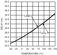
| tLPHL | Lower Turn-Off Propagation Delay LM5102 (LI Falling to LO Falling) |
27 | ns | |||
| –40°C to +125°C | 56 | |||||
| tHPHL | Upper Turn-Off Propagation Delay LM5102 (HI Falling to HO Falling) |
27 | ns | |||
| –40°C to +125°C | 56 | |||||
| tRC, tFC | Either Output Rise/Fall Time | CL = 1000 pF | 15 | ns | ||
| tR, tF | Either Output Rise/Fall Time (3 V to 9 V) | CL = 0.1 µF | 0.6 | µs | ||
| tBS | Bootstrap Diode Turn-Off Time | IF = 20 mA, IR = 200 mA | 50 | ns | ||
6.7 Typical Characteristics
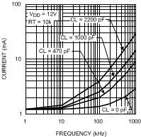
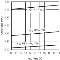
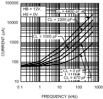
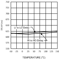
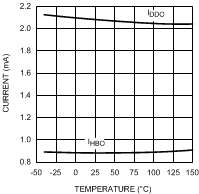
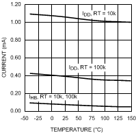
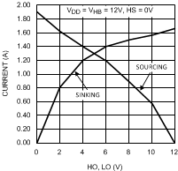

7 Detailed Description
7.1 Overview
The LM5102 device offers a unique flexibility with independently programmable delay of the rising edge for both high and low side driver outputs independently. The delays are set with resistors at the RT1 and RT2 pins, and can be adjusted from 100 ns to 600 ns. This feature reduces component count, board space and cost compared to discrete solutions for adjusting driver dead time. The wide delay programming range provides the flexibility to optimize drive signal timing for a wide range of MOSFETs and applications.
The RT pins are biased at 3 V and current limited to 1 mA maximum programming current. The time delay generator will accommodate resistor values from 5 k to 100 k with turn-on delay times that are proportional to the RT resistance. In addition, each RT pin is monitored by a comparator that will bypass the turn-on delay if the RT pin is pulled below the timer elimination threshold (1.8 V typical). Grounding the RT pins programs the LM5102 to drive both outputs with minimum turn-on delay.
7.2 Functional Block Diagram

7.3 Feature Description
7.3.1 Startup and UVLO
Both top and bottom drivers include undervoltage lockout (UVLO) protection circuitry which monitors the supply voltage (VDD) and bootstrap capacitor voltage (VHB – VHS) independently. The UVLO circuit inhibits each driver until sufficient supply voltage is available to turn-on the external MOSFETs, and the built-in hysteresis prevents chattering during supply voltage transitions. When the supply voltage is applied to VDD pin of LM5102, the top and bottom gates are held low until VDD exceeds UVLO threshold, typically about 6.9 V. Any UVLO condition on the bootstrap capacitor will disable only the high side output (HO).
7.4 Device Functional Modes
| LI Pin | LO Pin | HI Pin | HO Pin |
|---|---|---|---|
| L | L | L | L |
| H | H | H | H |