JAJSC52C April 2006 – September 2016 LM5109A
PRODUCTION DATA.
- 1 特長
- 2 アプリケーション
- 3 概要
- 4 改訂履歴
- 5 Pin Configuration and Functions
- 6 Specifications
- 7 Detailed Description
- 8 Application and Implementation
- 9 Power Supply Recommendations
- 10Layout
- 11デバイスおよびドキュメントのサポート
- 12メカニカル、パッケージ、および注文情報
パッケージ・オプション
メカニカル・データ(パッケージ|ピン)
サーマルパッド・メカニカル・データ
発注情報
6 Specifications
6.1 Absolute Maximum Ratings
See (1)(2)| MIN | MAX | UNIT | |
|---|---|---|---|
| VDD to VSS | –0.3 | 18 | V |
| HB to HS | −0.3 | 18 | V |
| LI or HI to VSS | −0.3 | VDD + 0.3 | V |
| LO to VSS | −0.3 | VDD + 0.3 | V |
| HO to VSS | VHS − 0.3 | VHB + 0.3 | V |
| HS to VSS(3) | −5 | 90 | V |
| HB to VSS | 108 | V | |
| Junction Temperature | –40 | 150 | °C |
| Storage Temperature Range | −55 | 150 | °C |
(1) Absolute Maximum Ratings indicate limits beyond which damage to the component may occur. Operating Ratings are conditions under which operation of the device is specified. Operating Ratings do not imply performance limits. For performance limits and associated test conditions, see the Electrical Characteristics.
(2) If Military/Aerospace specified devices are required, please contact the Texas Instruments Sales Office/Distributors for availability and specifications.
(3) In the application the HS node is clamped by the body diode of the external lower N-MOSFET, therefore the HS voltage will generally not exceed –1V. However in some applications, board resistance and inductance may result in the HS node exceeding this stated voltage transiently. If negative transients occur on HS, the HS voltage must never be more negative than VDD – 15V. For example, if VDD = 10V, the negative transients at HS must not exceed –5V.
6.2 ESD Ratings
| VALUE | UNIT | |||
|---|---|---|---|---|
| V(ESD) | Electrostatic discharge | Human-body model (HBM) (1) | ±1500 | V |
(1) The human body model is a 100 pF capacitor discharged through a 1.5kΩ resistor into each pin.
6.3 Recommended Operating Conditions
| MIN | NOM | MAX | UNIT | |
|---|---|---|---|---|
| VDD | 8 | 14 | V | |
| HS(1) | −1 | 90 | V | |
| HB | VHS + 8 | VHS + 14 | V | |
| HS Slew Rate | < 50 | V/ns | ||
| Junction Temperature | −40 | 125 | °C |
(1) In the application the HS node is clamped by the body diode of the external lower N-MOSFET, therefore the HS voltage will generally not exceed –1V. However in some applications, board resistance and inductance may result in the HS node exceeding this stated voltage transiently. If negative transients occur on HS, the HS voltage must never be more negative than VDD – 15V. For example, if VDD = 10V, the negative transients at HS must not exceed –5V.
6.4 Thermal Information
| THERMAL METRIC(1) | LM5109A | UNIT | ||
|---|---|---|---|---|
| D (SOIC) | NGT (WSON) | |||
| 8 PINS | 8 PINS | |||
| RθJA | Junction-to-ambient thermal resistance | 117.6 | 42.3 | °C/W |
| RθJC(top) | Junction-to-case (top) thermal resistance | 64.9 | 34 | °C/W |
| RθJB | Junction-to-board thermal resistance | 58.1 | 19.3 | °C/W |
| ψJT | Junction-to-top characterization parameter | 17.4 | 0.4 | °C/W |
| ψJB | Junction-to-board characterization parameter | 57.6 | 19.5 | °C/W |
| RθJC(bot) | Junction-to-case (bottom) thermal resistance | – | 8.1 | °C/W |
(1) For more information about traditional and new thermal metrics, see the Semiconductor and IC Package Thermal Metrics application report.
6.5 Electrical Characteristics
Unless otherwise specified, VDD = VHB = 12V, VSS = VHS = 0V, No Load on LO or HO(1). Typical limits are for TJ = 25°C, and minimum and maximum limits apply over the operating junction temperature range (–40°C to 125°C).| PARAMETER | TEST CONDITIONS | MIN | TYP | MAX | UNIT | |
|---|---|---|---|---|---|---|
| SUPPLY CURRENTS | ||||||
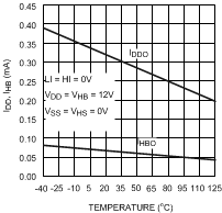
| IDD | VDD quiescent current | LI = HI = 0V | 0.3 | 0.6 | mA | |
| IDDO | VDD operating current | f = 500 kHz | 1.8 | 2.9 | mA | |
| IHB | Total HB quiescent current | LI = HI = 0V | 0.06 | 0.2 | mA | |
| IHBO | Total HB operating current | f = 500 kHz | 1.4 | 2.8 | mA | |
| IHBS | HB to VSS current, quiescent | VHS = VHB = 90V | 0.1 | 10 | µA | |
| IHBSO | HB to VSS current, operating | f = 500 kHz | 0.5 | mA | ||
| INPUT PINS LI and HI | ||||||
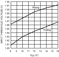
| VIL | Low-level input voltage threshold | 0.8 | 1.8 | V | ||
| VIH | High-level input voltage threshold | 1.8 | 2.2 | V | ||
| RI | Input pulldown resistance | 100 | 200 | 500 | kΩ | |
| UNDER-VOLTAGE PROTECTION | ||||||
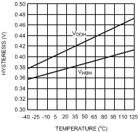
| VDDR | VDD rising threshold | VDDR = VDD – VSS | 6.0 | 6.7 | 7.4 | V |
| VDDH | VDD threshold hysteresis | 0.5 | V | |||
| VHBR | HB rising threshold | VHBR = VHB – VHS | 5.7 | 6.6 | 7.1 | V |
| VHBH | HB threshold hysteresis | 0.4 | V | |||
| LO GATE DRIVER | ||||||
| VOLL | Low-level output voltage | ILO = 100 mA, VOHL = VLO – VSS | 0.38 | 0.65 | V | |
| VOHL | High-level output voltage | ILO = −100 mA, VOHL = VDD – VLO | 0.72 | 1.20 | V | |
| IOHL | Peak pullup current | VLO = 0V | 1.0 | A | ||
| IOLL | Peak pulldown current | VLO = 12V | 1.0 | A | ||
| HO GATE DRIVER | ||||||
| VOLH | Low-level output voltage | IHO = 100 mA, VOLH = VHO – VHS | 0.38 | 0.65 | V | |
| VOHH | High-level output voltage | IHO = −100 mA, VOHH = VHB – VHO | 0.72 | 1.20 | V | |
| IOHH | Peak pullup current | VHO = 0V | 1.0 | A | ||
| IOLH | Peak pulldown current | VHO = 12V | 1.0 | A | ||
(1) Minimum and maximum limits are 100% production tested at 25°C. Limits over the operating temperature range are specified through correlation using Statistical Quality Control (SQC) methods. Limits are used to calculate Average Outgoing Quality Level (AOQL).
6.6 Switching Characteristics
Unless otherwise specified, VDD = VHB = 12V, VSS = VHS = 0V, No Load on LO or HO. Typical limits are for TJ = 25°C, and minimum and maximum limits apply over the operating junction temperature range (–40°C to 125°C).| PARAMETER | TEST CONDITIONS | MIN | TYP | MAX | UNIT | |
|---|---|---|---|---|---|---|
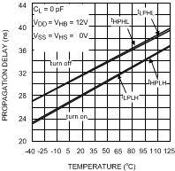
| tLPHL | Lower turn-off propagation delay (LI falling to LO falling) |
30 | 56 | ns | ||
| tHPHL | Upper turn-off propagation delay (HI falling to HO falling) |
30 | 56 | ns | ||
| tLPLH | Lower turn-on propagation delay (LI rising to LO rising) |
32 | 56 | ns | ||
| tHPLH | Upper turn-on propagation delay (HI rising to HO rising) |
32 | 56 | ns | ||
| tMON | Delay matching: lower turn-on and upper turn-off | 2 | 15 | ns | ||
| tMOFF | Delay matching: lower turn-off and upper turn-on | 2 | 15 | ns | ||
| tRC, tFC | Either output rise or fall time | CL = 1000 pF | 15 | - | ns | |
| tPW | Minimum input pulse width that changes the output | 50 | ns | |||
 Figure 1. Timing Diagram
6.7 Typical Performance Characteristics
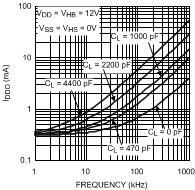

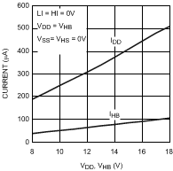

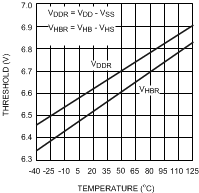
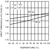

| VDD = VHB = 12 V | VSS = VHS = 0 V |
