JAJSC53C February 2007 – January 2016 LM5109B
PRODUCTION DATA.
- 1 特長
- 2 アプリケーション
- 3 概要
- 4 改訂履歴
- 5 Pin Configuration and Functions
- 6 Specifications
- 7 Detailed Description
- 8 Application and Implementation
- 9 Power Supply Recommendations
- 10Layout
- 11デバイスおよびドキュメントのサポート
- 12メカニカル、パッケージ、および注文情報
パッケージ・オプション
メカニカル・データ(パッケージ|ピン)
サーマルパッド・メカニカル・データ
発注情報
6 Specifications
6.1 Absolute Maximum Ratings
over operating free-air temperature range (unless otherwise noted)(1)| MIN | MAX | UNIT | |
|---|---|---|---|
| VDD to VSS | –0.3 | 18 | V |
| HB to HS | –0.3 | 18 | V |
| LI or HI to VSS | –0.3 | VDD + 0.3 | V |
| LO to VSS | –0.3 | VDD + 0.3 | V |
| HO to VSS | VHS – 0.3 | VHB + 0.3 | V |
| HS to VSS(2) | –5 | 90 | V |
| HB to VSS | 108 | V | |
| Junction temperature | –40 | 150 | °C |
| Storage temperature, Tstg | –55 | 150 | °C |
(1) Stresses beyond those listed under Absolute Maximum Ratings may cause permanent damage to the device. These are stress ratings only, which do not imply functional operation of the device at these or any other conditions beyond those indicated under Recommended Operating Conditions. Exposure to absolute-maximum-rated conditions for extended periods may affect device reliability.
(2) In the application the HS node is clamped by the body diode of the external lower N-MOSFET, therefore the HS voltage will generally not exceed –1 V. However in some applications, board resistance and inductance may result in the HS node exceeding this stated voltage transiently. If negative transients occur on HS, the HS voltage must never be more negative than VDD – 15 V. For example, if VDD = 10 V, the negative transients at HS must not exceed –5 V.
6.2 ESD Ratings
| VALUE | UNIT | |||
|---|---|---|---|---|
| V(ESD) | Electrostatic discharge | Human-body model (HBM), per ANSI/ESDA/JEDEC JS-001(1) | ±1500 | V |
| Charged-device model (CDM), per JEDEC specification JESD22-C101(2) | ±500 | |||
(1) JEDEC document JEP155 states that 500-V HBM allows safe manufacturing with a standard ESD control process.
(2) JEDEC document JEP157 states that 250-V CDM allows safe manufacturing with a standard ESD control process.
6.3 Recommended Operating Conditions
over operating free-air temperature range (unless otherwise noted)| MIN | MAX | UNIT | ||
|---|---|---|---|---|
| VDD | 8 | 14 | V | |
| HS(1) | –1 | 90 | V | |
| HB | VHS + 8 | VHS + 14 | V | |
| HS slew rate | 50 | V/ns | ||
| Junction temperature | –40 | 125 | °C | |
(1) In the application, the HS node is clamped by the body diode of the external lower N-MOSFET, therefore the HS voltage will generally not exceed –1 V. However in some applications, board resistance and inductance may result in the HS node exceeding this stated voltage transiently. If negative transients occur on HS, the HS voltage must never be more negative than VDD – 15 V. For example, if VDD = 10 V, the negative transients at HS must not exceed –5 V.
6.4 Thermal Information
| THERMAL METRIC(1) | LM5109B | UNIT | ||
|---|---|---|---|---|
| D (SOIC) | NGT (WSON) | |||
| 8 PINS | 8 PINS | |||
| RθJA | Junction-to-ambient thermal resistance | 117.6 | 42.3 | °C/W |
| RθJC(top) | Junction-to-case (top) thermal resistance | 64.9 | 34.0 | °C/W |
| RθJB | Junction-to-board thermal resistance | 58.1 | 19.3 | °C/W |
| ψJT | Junction-to-top characterization parameter | 17.4 | 0.4 | °C/W |
| ψJB | Junction-to-board characterization parameter | 57.6 | 19.5 | °C/W |
| RθJC(bot) | Junction-to-case (bottom) thermal resistance | – | 8.1 | °C/W |
(1) For more information about traditional and new thermal metrics, see the Semiconductor and IC Package Thermal Metrics application report, SPRA953.
6.5 Electrical Characteristics
TJ = 25°C (unless otherwise specified), VDD = VHB = 12 V, VSS = VHS = 0 V, No Load on LO or HO| PARAMETER | TEST CONDITIONS | MIN | TYP | MAX | UNIT | ||
|---|---|---|---|---|---|---|---|
| SUPPLY CURRENTS | |||||||
| IDD | VDD quiescent current | LI = HI = 0 V | TJ = 25°C | 0.3 | mA | ||
| TJ = –40°C to 125°C | 0.6 | ||||||
| IDDO | VDD operating current | f = 500 kHz | TJ = 25°C | 1.8 | mA | ||
| TJ = –40°C to 125°C | 2.9 | ||||||
| IHB | Total HB quiescent current | LI = HI = 0 V | TJ = 25°C | 0.06 | mA | ||
| TJ = –40°C to 125°C | 0.2 | ||||||
| IHBO | Total HB operating current | f = 500 kHz | TJ = 25°C | 1.4 | mA | ||
| TJ = –40°C to 125°C | 2.8 | ||||||
| IHBS | HB to VSS current, quiescent | VHS = VHB = 90 V | TJ = 25°C | 0.1 | µA | ||
| TJ = –40°C to 125°C | 10 | ||||||
| IHBSO | HB to VSS current, operating | f = 500 kHz | 0.5 | mA | |||
| INPUT PINS LI AND HI | |||||||
| VIL | Low level input voltage threshold | TJ = 25°C | 1.8 | V | |||
| TJ = –40°C to 125°C | 0.8 | ||||||
| VIH | High level input voltage threshold | TJ = 25°C | 1.8 | V | |||
| TJ = –40°C to 125°C | 2.2 | ||||||
| RI | Input pulldown resistance | TJ = 25°C | 200 | kΩ | |||
| TJ = –40°C to 125°C | 100 | 500 | |||||
| UNDERVOLTAGE PROTECTION | |||||||
| VDDR | VDD rising threshold | VDDR = VDD – VSS | TJ = 25°C | 6.7 | V | ||
| TJ = –40°C to 125°C | 6.0 | 7.4 | |||||
| VDDH | VDD threshold hysteresis | 0.5 | V | ||||
| VHBR | HB rising threshold | VHBR = VHB – VHS | TJ = 25°C | 6.6 | V | ||
| TJ = –40°C to 125°C | 5.7 | 7.1 | |||||
| VHBH | HB threshold hysteresis | 0.4 | V | ||||
| LO GATE DRIVER | |||||||
| VOLL | Low-level output voltage | ILO = 100 mA, VOHL = VLO – VSS | TJ = 25°C | 0.38 | V | ||
| TJ = –40°C to 125°C | 0.65 | ||||||
| VOHL | High-level output voltage | ILO = −100 mA, VOHL = VDD – VLO | TJ = 25°C | 0.72 | V | ||
| TJ = –40°C to 125°C | 1.2 | ||||||
| IOHL | Peak pullup current | VLO = 0 V | 1 | A | |||
| IOLL | Peak pulldown current | VLO = 12 V | 1 | A | |||
| HO GATE DRIVER | |||||||
| VOLH | Low-level output voltage | IHO = 100 mA, VOLH = VHO – VHS | TJ = 25°C | 0.38 | V | ||
| TJ = –40°C to 125°C | 0.65 | ||||||
| VOHH | High-level output voltage | IHO = −100 mA, VOHH = VHB – VHO | TJ = 25°C | 0.72 | V | ||
| TJ = –40°C to 125°C | 1.2 | ||||||
| IOHH | Peak pullup current | VHO = 0 V | 1 | A | |||
| IOLH | Peak pulldown current | VHO = 12 V | 1 | A | |||
6.6 Switching Characteristics
TJ = 25°C (unless otherwise specified), VDD = VHB = 12 V, VSS = VHS = 0 V, No Load on LO or HO| PARAMETER | TEST CONDITIONS | MIN | TYP | MAX | UNIT | |
|---|---|---|---|---|---|---|
| tLPHL | Lower turnoff propagation delay (LI falling to LO falling) |
TJ = 25°C | 30 | ns | ||
| TJ = –40°C to 125°C | 56 | |||||
| tHPHL | Upper turnoff propagation delay (HI falling to HO falling) |
TJ = 25°C | 30 | ns | ||
| TJ = –40°C to 125°C | 56 | |||||
| tLPLH | Lower turnon propagation delay (LI rising to LO rising) |
TJ = 25°C | 32 | ns | ||
| TJ = –40°C to 125°C | 56 | |||||
| tHPLH | Upper turnon propagation delay (HI rising to HO rising) |
TJ = 25°C | 32 | ns | ||
| TJ = –40°C to 125°C | 56 | |||||
| tMON | Delay matching: Lower turnon and upper turnoff | TJ = 25°C | 2 | ns | ||
| TJ = –40°C to 125°C | 15 | |||||
| tMOFF | Delay matching: Lower turnoff and upper turnon | TJ = 25°C | 2 | ns | ||
| TJ = –40°C to 125°C | 15 | |||||
| tRC, tFC | Either output rise and fall time | CL = 1000 pF | 15 | ns | ||
| tPW | Minimum input pulse width that changes the output | 50 | ns | |||
 Figure 1. Typical Test Timing Diagram
6.7 Typical Characteristics

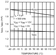
 Figure 4. Operating Current vs Temperature
 Figure 6. Quiescent Current vs Voltage
 Figure 8. LO and HO High Level Output Voltage
 vs Temperature
 Figure 10. Undervoltage Rising Thresholds
 vs Temperature
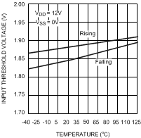
 Figure 12. Input Thresholds vs Temperature

| VDD = VHB = 12 V | VSS = VHS = 0 V |
 Figure 5. Quiescent Current vs Temperature
 Figure 7. Propagation Delay vs Temperature
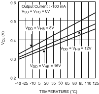
 Figure 9. LO and HO Low Level Output Voltage
 vs Temperature
 Figure 11. Undervoltage Hysteresis vs Temperature
 Figure 13. Input Thresholds vs Supply Voltage