JAJSBW4B May 2004 – September 2016 LM5110
PRODUCTION DATA.
8 Detailed Description
8.1 Overview
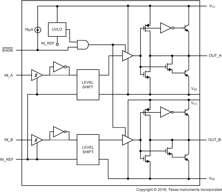
LM5110 dual gate driver consists of two independent and identical driver channels with TTL compatible logic inputs and high current totem-pole outputs that source or sink current to drive MOSFET gates. The driver output consist of a compound structure with MOS and bipolar transistor operating in parallel to optimize current capability over a wide output voltage and operating temperature range. The bipolar device provides high peak current at the critical threshold region of the MOSFET VGS while the MOS devices provide rail-to-rail output swing. The totem pole output drives the MOSFET gate between the gate drive supply voltage VCC and the power ground potential at the VEE pin.
The LM5110 is available in dual noninverting (-1), dual inverting (-2) and the combination inverting plus noninverting (-3) configurations. All three configurations are offered in the SOIC-8 and WSON-10 plastic packages.
8.2 Functional Block Diagram

8.3 Feature Description
8.3.1 Input Stage and Level Shifter
The control inputs of the drivers are high impedance CMOS buffers with TTL compatible threshold voltages. The negative supply of the input buffer is connected to the input ground pin IN_REF. An internal level shifting circuit connects the logic input buffers to the totem pole output drivers. The level shift circuit and separate input/output ground pins provide the option of single supply or split supply configurations. When driving MOSFET gates from a single positive supply, the IN_REF and VEE pins are both connected to the power ground. The LM5110 pinout was designed for compatibility with industry standard gate drivers in single supply gate driver applications. Pin 1 (IN_REF) on the LM5110 is a no-connect on standard driver IC's. Connecting pin 1 to pin 3 (VEE) on the printed-circuit board accommodates the pin-out of both the LM5110 and competitive drivers.
The input stage of each driver should be driven by a signal with a short rise and fall time. Slow rising and falling input signals, although not harmful to the driver, may result in the output switching repeatedly at a high frequency.
The input pins of noninverting drivers have an internal 18-μA current source pull-down to IN-REF. The input pins of inverting driver channels have neither pullup nor pulldown current sources. Unused input should be tied to IN_REF or VCC and not left open.
8.3.2 Output Stage
The two driver channels of the LM5110 are designed as identical cells. Transistor matching inherent to integrated circuit manufacturing ensures that the AC and DC performance of the channels are nearly identical. Closely matched propagation delays allow the dual driver to be operated as a single driver if inputs and output pins are connected. The drive current capability in parallel operation is 2X the drive of either channel. Small differences in switching speed between the driver channels will produce a transient current (shoot-through) in the output stage when two output pins are connected to drive a single load. Differences in input thresholds between the driver channels will also produce a transient current (shoot-through) in the output stage. Fast transition input signals are especially important while operating in a parallel configuration. The efficiency loss for parallel operation has been characterized at various loads, supply voltages and operating frequencies. The power dissipation in the LM5110 increases by less than 1% relative to the dual driver configuration when operated as a single driver with inputs and outputs connected.
8.3.3 Turn-off with Negative Bias
The isolated input/output grounds provide the capability to drive the MOSFET to a negative VGS voltage for a more robust and reliable off state. In split supply configuration, the IN_REF pin is connected to the ground of the controller which drives the LM5110 inputs. The VEE pin is connected to a negative bias supply that can range from the IN-REF as much as 14-V below the VCC gate drive supply.
Enhancement mode MOSFETs do not inherently require a negative bias on the gate to turn off the FET. However, certain applications may benefit from the capability of negative VGS voltage during turnoff including:
- When the gate voltages cannot be held safely below the threshold voltage due to transients or coupling in the printed-circuit-board.
- When driving low threshold MOSFETs at high junction temperatures.
- When high switching speeds produce capacitive gate-drain current that lifts the internal gate potential of the MOSFET.
8.3.4 UVLO and Power Supplies
An undervoltage lockout (UVLO) circuit is included in the LM5110, which senses the voltage difference between VCC and the input ground pin, IN_REF. When the VCC to IN_REF voltage difference falls below 2.7 V, both driver channels are disabled. The driver will resume normal operation when the VCC to IN_REF differential voltage exceeds approximately 2.9 V. UVLO hysteresis prevents chattering during brown-out conditions.
The maximum recommended voltage difference between VCC and IN_REF or between VCC and VEE is 14 V. The minimum voltage difference between VCC and IN_REF is 3.5 V.
8.3.5 Shutdown SHDN
The Shutdown pin (SHDN) is a TTL compatible logic input provided to enable/disable both driver channels. When SHDN is in the logic low state, the LM5110 is switched to a low power standby mode with total supply current less than 25 µA. This function can be effectively used for start-up, thermal overload, or short circuit fault protection. TI recommends connecting this pin to VCC when the shutdown function is not being used. The shutdown pin has an internal 18-μA current source pullup to VCC.
8.4 Device Functional Modes
The device operates in normal mode and UVLO mode. See Table 2 for more information on UVLO operation mode. In normal mode when the VCC and VIN–REF are above UVLO threshold, the output stage is dependent on the states of the IN_A, IN_B and nSHDN pins. The output HO and LO will be low if input state is floating.