SNVS790F January 2012 – November 2015 LM5114
PRODUCTION DATA.
- 1 Features
- 2 Applications
- 3 Description
- 4 Revision History
- 5 Device Comparison Table
- 6 Pin Configuration and Functions
- 7 Specifications
- 8 Detailed Description
- 9 Application and Implementation
- 10Power Supply Recommendations
- 11Layout
- 12Device and Documentation Support
- 13Mechanical, Packaging, and Orderable Information
パッケージ・オプション
メカニカル・データ(パッケージ|ピン)
サーマルパッド・メカニカル・データ
発注情報
1 Features
- Independent Source and Sink Outputs for Controllable Rise and Fall Times
- 4-V to 12.6-V Single Power Supply
- 7.6-A/1.3-A Peak Sink and Source Drive Current
- 0.23-Ω Open-drain Pulldown Sink Output
- 2-Ω Open-drain Pullup Source Output
- 12-ns (Typical) Propagation Delay
- Matching Delay Time Between Inverting and Noninverting Inputs
- TTL/CMOS Logic Inputs
- 0.68-V Input Hysteresis
- Up to 14-V Logic Inputs (Regardless of VDD Voltage)
- Low Input Capacitance: 2.5-pF (Typical)
- –40°C to 125°C Operating Temperature Range
- Pin-to-Pin Compatible With MAX5048
- 6-Pin SOT-23
2 Applications
- Boost Converters
- Flyback and Forward Converters
- Secondary Synchronous FETs Drive in Isolated Topologies
- Motor Control
3 Description
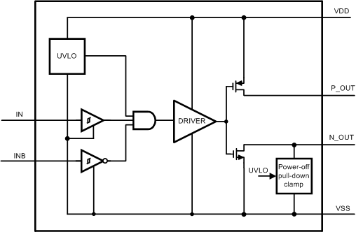
The LM5114 is designed to drive low-side MOSFETs in boost-type configurations or to drive secondary synchronous MOSFETs in isolated topologies. With strong sink current capability, the LM5114 can drive multiple FETs in parallel. The LM5114 also has the features necessary to drive low-side enhancement mode Gallium Nitride (GaN) FETs. The LM5114 provides inverting and noninverting inputs to satisfy requirements for inverting and Noninverting gate drive in a single device type. The inputs of the LM5114 are TTL/CMOS Logic compatible and withstand input voltages up to 14 V regardless of the VDD voltage. The LM5114 has split gate outputs, providing flexibility to adjust the turnon and turnoff strength independently. The LM5114 has fast switching speed and minimized propagation delays, facilitating high-frequency operation. The LM5114 is available in a 6-pin SOT-23 package and a 6-pin WSON package with an exposed pad to aid thermal dissipation.
Device Information(1)
| PART NUMBER | PACKAGE | BODY SIZE (NOM) |
|---|---|---|
| LM5114 | SOT-23 (6) | 2.90 mm × 1.60 mm |
| WSON (6) | 3.00 mm × 3.00 mm |
- For all available packages, see the orderable addendum at the end of the data sheet.
Block Diagram
