JAJSB27I August 2010 – April 2018 LM5119
PRODUCTION DATA.
- 1 特長
- 2 アプリケーション
- 3 概要
- 4 改訂履歴
- 5 Pin Configuration and Functions
- 6 Specifications
-
7 Detailed Description
- 7.1 Overview
- 7.2 Functional Block Diagram
- 7.3
Feature Description
- 7.3.1 High Voltage Start-Up Regulator
- 7.3.2 UVLO
- 7.3.3 Enable 2
- 7.3.4 Oscillator and Sync Capability
- 7.3.5 Error Amplifiers and PWM Comparators
- 7.3.6 Ramp Generator
- 7.3.7 Current Limit
- 7.3.8 Hiccup Mode Current Limiting
- 7.3.9 Soft Start
- 7.3.10 HO and LO Output Drivers
- 7.3.11 Maximum Duty Cycle
- 7.3.12 Thermal Protection
- 7.4 Device Functional Modes
-
8 Application and Implementation
- 8.1 Application Information
- 8.2
Typical Applications
- 8.2.1
Dual-output Design Example
- 8.2.1.1 Design Requirements
- 8.2.1.2
Detailed Design Procedure
- 8.2.1.2.1 Timing Resistor
- 8.2.1.2.2 Output Inductor
- 8.2.1.2.3 Current Sense Resistor
- 8.2.1.2.4 Ramp Resistor and Ramp Capacitor
- 8.2.1.2.5 Output Capacitors
- 8.2.1.2.6 Input Capacitors
- 8.2.1.2.7 VCC Capacitor
- 8.2.1.2.8 Bootstrap Capacitor
- 8.2.1.2.9 Soft-Start Capacitor
- 8.2.1.2.10 Restart Capacitor
- 8.2.1.2.11 Output Voltage Divider
- 8.2.1.2.12 UVLO Divider
- 8.2.1.2.13 MOSFET Snubber
- 8.2.1.2.14 Error Amplifier Compensation
- 8.2.1.3 Application Curves
- 8.2.2 Two-Phase Design Example
- 8.2.1
Dual-output Design Example
- 9 Power Supply Recommendations
- 10Layout
- 11デバイスおよびドキュメントのサポート
- 12メカニカル、パッケージ、および注文情報
パッケージ・オプション
メカニカル・データ(パッケージ|ピン)
- RTV|32
サーマルパッド・メカニカル・データ
- RTV|32
発注情報
8.2.1.2.2 Output Inductor
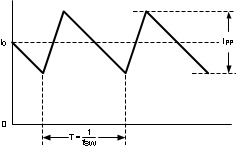
The inductor value is determined based on the operating frequency, load current, ripple current, and the input and output voltages.
 Figure 15. Inductor Current
Knowing the switching frequency, maximum ripple current (IPP), maximum input voltage, and the nominal output voltage (VOUT), the inductor value can be calculated with Equation 8.

The maximum ripple current occurs at the maximum input voltage. Typically, IPP is 20% to 40% of the full load current. When operating in the diode emulation mode configuration, the maximum ripple current must be less than twice the minimum load current. For full synchronous operation, higher ripple current is acceptable. Higher ripple current allows for a smaller inductor size, but places more of a burden on the output capacitor to smooth the ripple current. For the example in Equation 9, a ripple current of 15% of 8 A was chosen as a compromise for the 10-V output.

The nearest standard value of 15 μH was chosen for L. Using the value of 15 µH for L in Equation 10 as the example (Equation 11), calculate IPP again. This step is necessary if the chosen value of L differs significantly from the calculated value.

