JAJSFD4A May 2018 – November 2018 LM5122ZA
PRODUCTION DATA.
- 1 特長
- 2 アプリケーション
- 3 概要
- 4 改訂履歴
- 5 概要(続き)
- 6 Pin Configuration and Functions
- 7 Specifications
-
8 Detailed Description
- 8.1 Overview
- 8.2 Functional Block Diagram
- 8.3
Feature Description
- 8.3.1 Undervoltage Lockout (UVLO)
- 8.3.2 High-Voltage VCC Regulator
- 8.3.3 Oscillator
- 8.3.4 Slope Compensation
- 8.3.5 Error Amplifier
- 8.3.6 PWM Comparator
- 8.3.7 Soft Start
- 8.3.8 HO and LO Drivers
- 8.3.9 Bypass Operation (VOUT = VIN)
- 8.3.10 Cycle-by-Cycle Current Limit
- 8.3.11 Clock Synchronization
- 8.3.12 Maximum Duty Cycle
- 8.3.13 Thermal Protection
- 8.4 Device Functional Modes
-
9 Application and Implementation
- 9.1
Application Information
- 9.1.1 Feedback Compensation
- 9.1.2 Sub-Harmonic Oscillation
- 9.1.3 Interleaved Boost Configuration
- 9.1.4 DCR Sensing
- 9.1.5 Output Overvoltage Protection
- 9.1.6 SEPIC Converter Simplified Schematic
- 9.1.7 Non-Isolated Synchronous Flyback Converter Simplified Schematic
- 9.1.8 Negative to Positive Conversion
- 9.2
Typical Application
- 9.2.1 Design Requirements
- 9.2.2
Detailed Design Procedure
- 9.2.2.1 Timing Resistor RT
- 9.2.2.2 UVLO Divider RUV2, RUV1
- 9.2.2.3 Input Inductor LIN
- 9.2.2.4 Current Sense Resistor RS
- 9.2.2.5 Current Sense Filter RCSFP, RCSFN, CCS
- 9.2.2.6 Slope Compensation Resistor RSLOPE
- 9.2.2.7 Output Capacitor COUT
- 9.2.2.8 Input Capacitor CIN
- 9.2.2.9 VIN Filter RVIN, CVIN
- 9.2.2.10 Bootstrap Capacitor CBST and Boost Diode DBST
- 9.2.2.11 VCC Capacitor CVCC
- 9.2.2.12 Output Voltage Divider RFB1, RFB2
- 9.2.2.13 Soft-Start Capacitor CSS
- 9.2.2.14 Restart Capacitor CRES
- 9.2.2.15 Low-Side Power Switch QL
- 9.2.2.16 High-Side Power Switch QH and Additional Parallel Schottky Diode
- 9.2.2.17 Snubber Components
- 9.2.2.18 Loop Compensation Components CCOMP, RCOMP, CHF
- 9.2.3 Application Curves
- 9.1
Application Information
- 10Power Supply Recommendations
- 11Layout
- 12デバイスおよびドキュメントのサポート
- 13メカニカル、パッケージ、および注文情報
パッケージ・オプション
メカニカル・データ(パッケージ|ピン)
- PWP|24
サーマルパッド・メカニカル・データ
- PWP|24
発注情報
8.3.1 Undervoltage Lockout (UVLO)
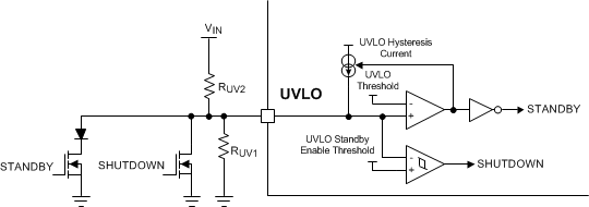
The LM5122ZA features a dual level UVLO circuit. When the UVLO pin voltage is less than the 0.4-V UVLO standby enable threshold, the LM5122ZA is in the shutdown mode with all functions disabled. The shutdown comparator provides 0.1 V of hysteresis to avoid chatter during transition. If the UVLO pin voltage is greater than 0.4 V and below 1.2 V during power up, the controller is in standby mode with the VCC regulator operational and no switching at the HO and LO outputs. This feature allows the UVLO pin to be used as a remote shutdown function by pulling the UVLO pin down below the UVLO standby enable threshold with an external open collector or open drain device.
 Figure 16. UVLO Remote Standby and Shutdown Control
 If the UVLO pin voltage is above the 1.2-V UVLO threshold and VCC voltage exceeds the VCC UV threshold, a start-up sequence begins. UVLO hysteresis is accomplished with an internal 10-μA current source that is switched on or off into the impedance of the UVLO setpoint divider. When the UVLO pin voltage exceeds 1.2 V, the current source is enabled to quickly raise the voltage at the UVLO pin. When the UVLO pin voltage falls below the 1.2-V UVLO threshold, the current source is disabled causing the voltage at the UVLO pin to quickly fall. In addition to the UVLO hysteresis current source, a 5-μs deglitch filter on both rising and falling edge of UVLO toggling helps preventing chatter upon power up or down.
An external UVLO setpoint voltage divider from the supply voltage to AGND is used to set the minimum input operating voltage of the regulator. The divider must be designed such that the voltage at the UVLO pin is greater than 1.2 V when the input voltage is in the desired operating range. The maximum voltage rating of the UVLO pin is 15 V. If necessary, the UVLO pin can be clamped with an external zener diode. The UVLO pin should not be left floating. The values of RUV1 and RUV2 can be determined from Equation 1 and Equation 2.


where
- VHYS is the desired UVLO hysteresis
- VIN(STARTUP) is the desired startup voltage of the regulator during turn-on.
Typical shutdown voltage during turn-off can be calculated as follows:
