JAJSFD4A May 2018 – November 2018 LM5122ZA
PRODUCTION DATA.
- 1 特長
- 2 アプリケーション
- 3 概要
- 4 改訂履歴
- 5 概要(続き)
- 6 Pin Configuration and Functions
- 7 Specifications
-
8 Detailed Description
- 8.1 Overview
- 8.2 Functional Block Diagram
- 8.3
Feature Description
- 8.3.1 Undervoltage Lockout (UVLO)
- 8.3.2 High-Voltage VCC Regulator
- 8.3.3 Oscillator
- 8.3.4 Slope Compensation
- 8.3.5 Error Amplifier
- 8.3.6 PWM Comparator
- 8.3.7 Soft Start
- 8.3.8 HO and LO Drivers
- 8.3.9 Bypass Operation (VOUT = VIN)
- 8.3.10 Cycle-by-Cycle Current Limit
- 8.3.11 Clock Synchronization
- 8.3.12 Maximum Duty Cycle
- 8.3.13 Thermal Protection
- 8.4 Device Functional Modes
-
9 Application and Implementation
- 9.1
Application Information
- 9.1.1 Feedback Compensation
- 9.1.2 Sub-Harmonic Oscillation
- 9.1.3 Interleaved Boost Configuration
- 9.1.4 DCR Sensing
- 9.1.5 Output Overvoltage Protection
- 9.1.6 SEPIC Converter Simplified Schematic
- 9.1.7 Non-Isolated Synchronous Flyback Converter Simplified Schematic
- 9.1.8 Negative to Positive Conversion
- 9.2
Typical Application
- 9.2.1 Design Requirements
- 9.2.2
Detailed Design Procedure
- 9.2.2.1 Timing Resistor RT
- 9.2.2.2 UVLO Divider RUV2, RUV1
- 9.2.2.3 Input Inductor LIN
- 9.2.2.4 Current Sense Resistor RS
- 9.2.2.5 Current Sense Filter RCSFP, RCSFN, CCS
- 9.2.2.6 Slope Compensation Resistor RSLOPE
- 9.2.2.7 Output Capacitor COUT
- 9.2.2.8 Input Capacitor CIN
- 9.2.2.9 VIN Filter RVIN, CVIN
- 9.2.2.10 Bootstrap Capacitor CBST and Boost Diode DBST
- 9.2.2.11 VCC Capacitor CVCC
- 9.2.2.12 Output Voltage Divider RFB1, RFB2
- 9.2.2.13 Soft-Start Capacitor CSS
- 9.2.2.14 Restart Capacitor CRES
- 9.2.2.15 Low-Side Power Switch QL
- 9.2.2.16 High-Side Power Switch QH and Additional Parallel Schottky Diode
- 9.2.2.17 Snubber Components
- 9.2.2.18 Loop Compensation Components CCOMP, RCOMP, CHF
- 9.2.3 Application Curves
- 9.1
Application Information
- 10Power Supply Recommendations
- 11Layout
- 12デバイスおよびドキュメントのサポート
- 13メカニカル、パッケージ、および注文情報
パッケージ・オプション
メカニカル・データ(パッケージ|ピン)
- PWP|24
サーマルパッド・メカニカル・データ
- PWP|24
発注情報
8.3.11 Clock Synchronization
The SYNCIN/RT pin can be used to synchronize the internal oscillator to an external clock. A positive going synchronization clock at the RT pin must exceed the RT sync rising threshold and negative going synchronization clock at RT pin must exceed the RT sync falling threshold to trip the internal synchronization pulse detector.
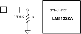
In Master1 mode, two types of configurations are allowed for clock synchronization. With the configuration in Figure 23, the frequency of the external synchronization pulse is recommended to be within +40% and –20% of the internal oscillator frequency programmed by the RT resistor. For example, 900-kHz external synchronization clock and 20-kΩ RT resistor are required for 450-kHz switching in master1 mode. The internal oscillator can be synchronized by AC coupling a positive edge into the RT pin. A 5-V amplitude pulse signal coupled through 100-pF capacitor is a good starting point. The RT resistor is always required with AC coupling capacitor with the Figure 23 configuration, whether the oscillator is free running or externally synchronized.
Care should be taken to ensure that the RT pin voltage does not go below –0.3 V at the falling edge of the external pulse. This may limit the duty cycle of external synchronization pulse. There is approximately 400-ns delay from the rising edge of the external pulse to the rising edge of LO.
 Figure 23. Oscillator Synchronization Through AC Coupling in Master1 Mode
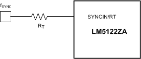
 With the configuration in Figure 24, the internal oscillator can be synchronized by connecting the external synchronization clock into the RT pin through RT resistor with free of the duty cycle limit. The output stage of the external clock source should be a low impedance totem-pole structure. Default logic state of fSYNC must be low.
 Figure 24. Oscillator Synchronization Through a Resistor in Master1 Mode
 In master2 and slave modes, connect this external synchronization clock directly to the RT pin and always provide continuously. The internal oscillator frequency can be either of two times faster than switching frequency or the same as the switching frequency by configuring the combination of FB and OPT pins (see Table 1).