JAJSGF1C October 2018 – June 2021 LM5143-Q1
PRODUCTION DATA
- 1 特長
- 2 アプリケーション
- 3 概要
- 4 Revision History
- 5 概要 (続き)
- 6 Pin Configuration and Functions
- 7 Specifications
-
8 Detailed Description
- 8.1 Overview
- 8.2 Functional Block Diagram
- 8.3
Feature Description
- 8.3.1 Input Voltage Range (VIN)
- 8.3.2 High-Voltage Bias Supply Regulator (VCC, VCCX, VDDA)
- 8.3.3 Enable (EN1, EN2)
- 8.3.4 Power Good Monitor (PG1, PG2)
- 8.3.5 Switching Frequency (RT)
- 8.3.6 Clock Synchronization (DEMB)
- 8.3.7 Synchronization Out (SYNCOUT)
- 8.3.8 Spread Spectrum Frequency Modulation (DITH)
- 8.3.9 Configurable Soft Start (SS1, SS2)
- 8.3.10 Output Voltage Setpoint (FB1, FB2)
- 8.3.11 Minimum Controllable On-Time
- 8.3.12 Error Amplifier and PWM Comparator (FB1, FB2, COMP1, COMP2)
- 8.3.13 Slope Compensation
- 8.3.14 Inductor Current Sense (CS1, VOUT1, CS2, VOUT2)
- 8.3.15 Hiccup Mode Current Limiting (RES)
- 8.3.16 High-Side and Low-Side Gate Drivers (HO1/2, LO1/2, HOL1/2, LOL1/2)
- 8.3.17 Output Configurations (MODE, FB2)
- 8.4 Device Functional Modes
-
9 Application and Implementation
- 9.1 Application Information
- 9.2 Typical Applications
- 10Power Supply Recommendations
- 11Layout
- 12Device and Documentation Support
- 13Mechanical, Packaging, and Orderable Information
8.3.17.1 Independent Dual-Output Operation
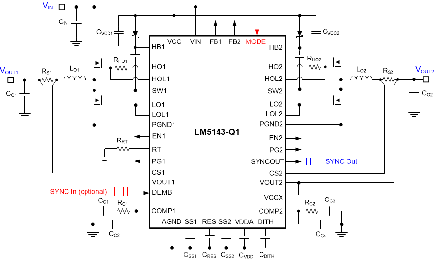
The LM5143-Q1 has two outputs that can operate independently. Both VOUT1 and VOUT2 can be set at 3.3 V or 5 V without installing external feedback resistors. Alternatively, set the output voltages between 0.6 V to 55 V using external feedback resistors based on Equation 5. See Table 8-1 and Figure 8-8. Connect MODE directly to AGND for independent outputs.
Table 8-1 Output Voltage Settings
| MODE | FB1 | FB2 | VOUT1 | VOUT2 | ERROR AMPLIFIER gm |
|---|---|---|---|---|---|
| AGND | AGND | AGND | 5 V | 5 V | 1200 µS |
| AGND | VDDA | VDDA | 3.3 V | 3.3 V | 1200 µS |
| AGND | VDDA | AGND | 3.3 V | 5 V | 1200 µS |
| AGND | AGND | VDDA | 5 V | 3.3 V | 1200 µS |
| AGND | Rdivider | Rdivider | 0.6 V to 55 V | 0.6 V to 55 V | 1200 µS |
| 10 kΩ to AGND | AGND | AGND | 5 V | 5 V | 60 µS |
| 10 kΩ to AGND | VDDA | VDDA | 3.3 V | 3.3 V | 60 µS |
| 10 kΩ to AGND | VDDA | AGND | 3.3 V | 5 V | 60 µS |
| 10 kΩ to AGND | AGND | VDDA | 5 V | 3.3 V | 60 µS |
| 10 kΩ to AGND | Rdivider | Rdivider | 0.6 V to 55 V | 0.6 V to 55 V | 60 µS |
 Figure 8-8 Regulator Schematic Configured for Independent Dual Outputs