JAJSGF1C October 2018 – June 2021 LM5143-Q1
PRODUCTION DATA
- 1 特長
- 2 アプリケーション
- 3 概要
- 4 Revision History
- 5 概要 (続き)
- 6 Pin Configuration and Functions
- 7 Specifications
-
8 Detailed Description
- 8.1 Overview
- 8.2 Functional Block Diagram
- 8.3
Feature Description
- 8.3.1 Input Voltage Range (VIN)
- 8.3.2 High-Voltage Bias Supply Regulator (VCC, VCCX, VDDA)
- 8.3.3 Enable (EN1, EN2)
- 8.3.4 Power Good Monitor (PG1, PG2)
- 8.3.5 Switching Frequency (RT)
- 8.3.6 Clock Synchronization (DEMB)
- 8.3.7 Synchronization Out (SYNCOUT)
- 8.3.8 Spread Spectrum Frequency Modulation (DITH)
- 8.3.9 Configurable Soft Start (SS1, SS2)
- 8.3.10 Output Voltage Setpoint (FB1, FB2)
- 8.3.11 Minimum Controllable On-Time
- 8.3.12 Error Amplifier and PWM Comparator (FB1, FB2, COMP1, COMP2)
- 8.3.13 Slope Compensation
- 8.3.14 Inductor Current Sense (CS1, VOUT1, CS2, VOUT2)
- 8.3.15 Hiccup Mode Current Limiting (RES)
- 8.3.16 High-Side and Low-Side Gate Drivers (HO1/2, LO1/2, HOL1/2, LOL1/2)
- 8.3.17 Output Configurations (MODE, FB2)
- 8.4 Device Functional Modes
-
9 Application and Implementation
- 9.1 Application Information
- 9.2 Typical Applications
- 10Power Supply Recommendations
- 11Layout
- 12Device and Documentation Support
- 13Mechanical, Packaging, and Orderable Information
7.7 Typical Characteristics
VIN = VEN1 = VEN2 = 12 V, TJ = 25°C, unless otherwise stated.
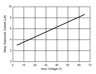
| VEN1 = VEN2 = 0 V |
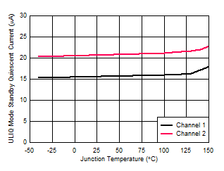 Figure 7-9 ULIQ Mode Standby Current versus Temperature
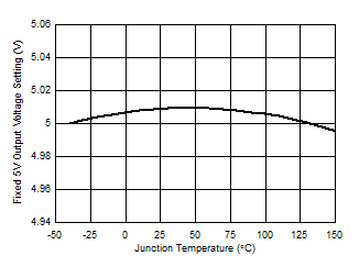 Figure 7-11 Fixed 5-V Output Voltage (VOUT1) versus Temperature
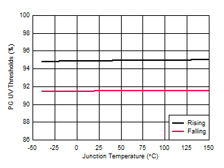 Figure 7-13 PG UV Thresholds versus Temperature
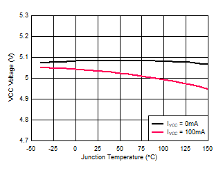 Figure 7-15 VCC Regulation Voltage versus Temperature
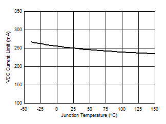 Figure 7-17 VCC Current Limit versus Temperature
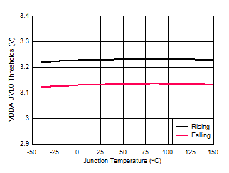 Figure 7-19 VDDA UVLO Thresholds versus Temperature
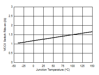 Figure 7-21 VCCX Switch Resistance versus Temperature
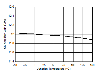 Figure 7-23 Current Sense (CS1) Amplifier Gain versus Temperature
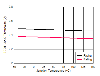 Figure 7-25 BOOT (HB1) UVLO Thresholds versus Temperature
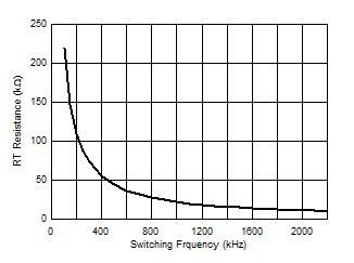 Figure 7-27 RT Resistance versus Switching Frequency
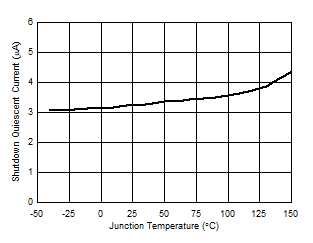
| VEN1 = VEN2 = 0 V |
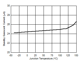
| VEN2 = 0 V |
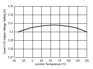 Figure 7-10 Fixed 3.3-V Output Voltage (VOUT1) versus Temperature
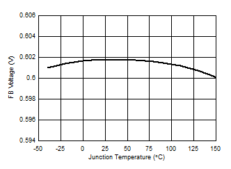 Figure 7-12 Feedback Voltage versus Temperature
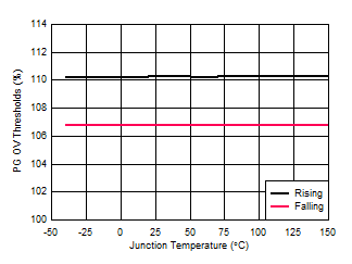 Figure 7-14 PG OV Thresholds versus Temperature
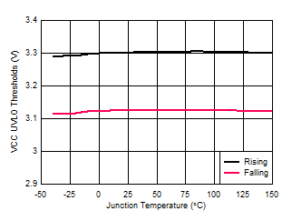 Figure 7-16 VCC UVLO Thresholds versus Temperature
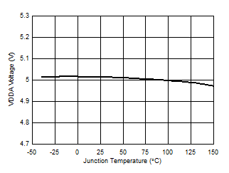 Figure 7-18 VDDA Regulation Voltage versus Temperature
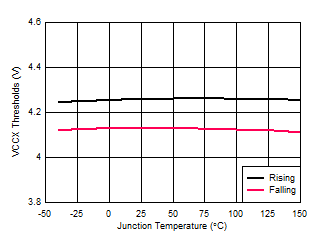 Figure 7-20 VCCX On/Off Thresholds versus Temperature
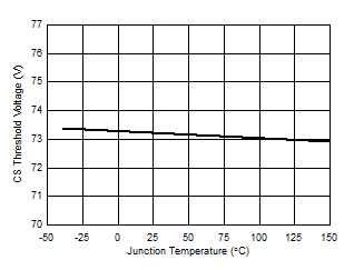 Figure 7-22 Current Sense (CS1) Threshold versus Temperature
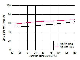 Figure 7-24 Minimum On Time and Off Time (HO1) versus Temperature
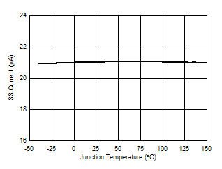 Figure 7-26 Soft-start (SS1) Current versus Temperature
