JAJSDA5B November   2017  – November 2020 LM5145

PRODUCTION DATA  

  1. 特長
  2. アプリケーション
  3. 概要
  4. Revision History
  5. Description (continued)
  6. Pin Configuration and Functions
    1. 6.1 Wettable Flanks
  7. Specifications
    1. 7.1 Absolute Maximum Ratings
    2. 7.2 ESD Ratings
    3. 7.3 Recommended Operating Conditions
    4. 7.4 Thermal Information
    5. 7.5 Electrical Characteristics
    6. 7.6 Switching Characteristics
    7. 7.7 Typical Characteristics
  8. Detailed Description
    1. 8.1 Overview
    2. 8.2 Functional Block Diagram
    3. 8.3 Feature Description
      1. 8.3.1  Input Range (VIN)
      2. 8.3.2  Output Voltage Setpoint and Accuracy (FB)
      3. 8.3.3  High-Voltage Bias Supply Regulator (VCC)
      4. 8.3.4  Precision Enable (EN/UVLO)
      5. 8.3.5  Power Good Monitor (PGOOD)
      6. 8.3.6  Switching Frequency (RT, SYNCIN)
        1. 8.3.6.1 Frequency Adjust
        2. 8.3.6.2 Clock Synchronization
      7. 8.3.7  Configurable Soft Start (SS/TRK)
        1. 8.3.7.1 Tracking
      8. 8.3.8  Voltage-Mode Control (COMP)
      9. 8.3.9  Gate Drivers (LO, HO)
      10. 8.3.10 Current Sensing and Overcurrent Protection (ILIM)
      11. 8.3.11 OCP Duty Cycle Limiter
    4. 8.4 Device Functional Modes
      1. 8.4.1 Shutdown Mode
      2. 8.4.2 Standby Mode
      3. 8.4.3 Active Mode
      4. 8.4.4 Diode Emulation Mode
      5. 8.4.5 Thermal Shutdown
  9. Application and Implementation
    1. 9.1 Application Information
      1. 9.1.1 Design and Implementation
      2. 9.1.2 Power Train Components
        1. 9.1.2.1 Inductor
        2. 9.1.2.2 Output Capacitors
        3. 9.1.2.3 Input Capacitors
        4. 9.1.2.4 Power MOSFETs
      3. 9.1.3 Control Loop Compensation
      4. 9.1.4 EMI Filter Design
    2. 9.2 Typical Applications
      1. 9.2.1 Design 1 – 20-A High-Efficiency Synchronous Buck Regulator for Telecom Power Applications
        1. 9.2.1.1 Design Requirements
        2. 9.2.1.2 Detailed Design Procedure
        3. 9.2.1.3 Custom Design With WEBENCH® Tools
        4. 9.2.1.4 Application Curves
      2. 9.2.2 Design 2 – High Density, 12-V, 10-A Rail With LDO Low-Noise Auxiliary Output for RF Power Applications
        1. 9.2.2.1 Design Requirements
        2. 9.2.2.2 Detailed Design Procedure
        3. 9.2.2.3 Application Curves
      3. 9.2.3 Design 3 – 150-W, Regulated 24-V Rail for Commercial Drone Applications With Output Voltage Tracking Feature
        1. 9.2.3.1 Design Requirements
        2. 9.2.3.2 Detailed Design Procedure
        3. 9.2.3.3 Application Curves
      4. 9.2.4 Design 4 – Powering a Multicore DSP From a 24-V or 48-V Rail
        1. 9.2.4.1 Design Requirements
        2. 9.2.4.2 Detailed Design Procedure
        3. 9.2.4.3 Application Curves
  10. 10Power Supply Recommendations
  11. 11Layout
    1. 11.1 Layout Guidelines
      1. 11.1.1 Power Stage Layout
      2. 11.1.2 Gate Drive Layout
      3. 11.1.3 PWM Controller Layout
      4. 11.1.4 Thermal Design and Layout
      5. 11.1.5 Ground Plane Design
    2. 11.2 Layout Example
  12. 12Device and Documentation Support
    1. 12.1 Device Support
      1. 12.1.1 Third-Party Products Disclaimer
      2. 12.1.2 Development Support
      3. 12.1.3 Custom Design With WEBENCH® Tools
    2. 12.2 Documentation Support
      1. 12.2.1 Related Documentation
        1. 12.2.1.1 PCB Layout Resources
        2. 12.2.1.2 Thermal Design Resources
    3. 12.3 Receiving Notification of Documentation Updates
    4. 12.4 Support Resources
    5. 12.5 Trademarks
    6. 12.6 Electrostatic Discharge Caution
    7. 12.7 Glossary
  13. 13Mechanical, Packaging, and Orderable Information

パッケージ・オプション

デバイスごとのパッケージ図は、PDF版データシートをご参照ください。

メカニカル・データ(パッケージ|ピン)
  • RGY|20
サーマルパッド・メカニカル・データ
発注情報

Typical Characteristics

VVIN = 48 V, RRT = 25 kΩ, SYNCIN tied to VCC, EN/UVLO tied to VIN (unless otherwise noted).
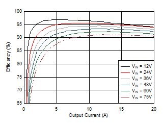
GUID-8CBEE320-F21F-4B36-9899-2CF818BE888B-low.gif
VOUT = 5 V VSYNCIN = VVCC FSW = 230 kHz
See Figure 9-5 RRT = 43.2 kΩ
Figure 7-1 Efficiency vs Load, CCM
GUID-1E4D3F02-92D0-464D-B602-62428D907670-low.gif
VOUT = 12 V FSW = 400 kHz
See Figure 9-20 RRT = 24.9 kΩ
Figure 7-3 Efficiency vs Load, CCM
GUID-AB369237-BCC6-4692-A631-9030ABEDC64A-low.gif
VOUT = 1.1 V FSW = 300 kHz
See Figure 9-46 RRT = 33.2 kΩ
Figure 7-5 Efficiency vs Load, CCM
GUID-41B4784E-8FA5-4B78-9026-2D44E2C211F5-low.gif
 
Figure 7-7 tON(min) and tOFF(min) vs Junction Temperature
GUID-B34063B2-1C13-4A8C-9CF1-CCB604487343-low.gif
VSW = 0 V VEN/UVLO = 1 V
Figure 7-9 IQ-STANDBY vs Input Voltage
GUID-C851BDBF-BEC9-4A74-B787-9FBA7DA855B3-low.gif
VSW = 0 V HO, LO Open
Figure 7-11 IQ-OPERATING (Switching) vs Input Voltage
GUID-20E189F5-5D6A-440B-875E-EBFD038A9355-low.gif
 
Figure 7-13 ILIM Current Source vs Junction Temperature
GUID-CBDAFB7A-7624-45A7-8F61-383025F00ACE-low.gifFigure 7-15 VCC UVLO Thresholds vs Junction Temperature
GUID-E9D2AEE7-07AD-4447-B788-E32D9B634942-low.gifFigure 7-17 PGOOD UVP Thresholds vs Junction Temperature
GUID-CCF8A686-1686-4382-A583-C956D9EE05AB-low.gifFigure 7-19 EN/UVLO Threshold vs Junction Temperature
GUID-7681B1AA-5163-45F8-A491-FF895660D375-low.gif
VSW = 0 V
Figure 7-21 Oscillator Frequency vs RT Resistance
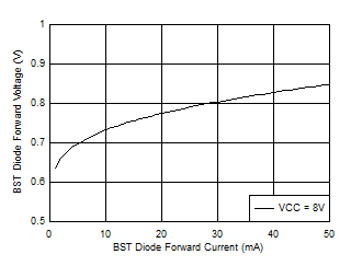
GUID-DB5D1971-B3CF-4D6D-ABF6-B1F97EB1C352-low.gifFigure 7-23 BST Diode Forward Voltage vs Current
GUID-071DF25C-6023-4F8C-9FC3-6DC647D8A889-low.gifFigure 7-25 HO Driver Resistance vs VCC Voltage
GUID-C6A6631C-018F-4C54-B78E-B4688C722A95-low.gif
VSS/TRK = 0 V
Figure 7-27 VCC Voltage vs Input Voltage
GUID-84DEAE23-868C-494A-A3F8-E188E8FF0E40-low.gif
VIN = 12 V
Figure 7-29 VCC vs ICC Characteristic
GUID-253E1A2D-6F6C-4A8D-9B8C-59B6F9ED37B9-low.gif
VOUT = 5 V VSYNCIN = 0 V FSW = 230 kHz
See Figure 9-5 RRT = 43.2 kΩ
Figure 7-2 Efficiency vs Load, DCM
GUID-B9CEBA85-D27E-4ADC-8B05-B2FADBCD0B18-low.gif
VOUT = 24 V FSW = 440 kHz
See Figure 9-33 RRT = 22.6 kΩ
Figure 7-4 Efficiency vs Load, CCM
GUID-761F3E56-8ED2-44D5-9C2C-3A5A39CFE68A-low.gif
  
Figure 7-6 FB Voltage vs Junction Temperature
GUID-1811D3C0-E492-4E2A-98DB-B1746DA3A010-low.gif
VSW = 0 V VEN/UVLO = 0 V
Figure 7-8 IQ-SHD vs Input Voltage
GUID-02F24256-DD28-40E5-BD3A-1AD8E56B5C88-low.gif
VSW = 0 V VEN/UVLO = VVIN VSS/TRK = 0 V
Figure 7-10 IQ-OPERATING (Non-switching) vs Input Voltage
GUID-CA8C0823-B8B9-4D18-A5A1-963A8F89F893-low.gif
VSW = 0 V VVCC = VBST = VILIM VFB = 0 V
Figure 7-12 VIN Quiescent Current With External VCC Applied
GUID-4ED93EC1-834A-4596-8D97-0BA15ED59510-low.gif
VSW = 0 V
Figure 7-14 Deadtime vs Junction Temperature
GUID-47390589-0E0B-4776-9DC1-F177C6AC263C-low.gifFigure 7-16 BST UVLO Thresholds vs Junction Temperature
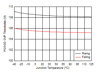
GUID-FA5893DB-94EE-4C15-8698-B241F569932C-low.gifFigure 7-18 PGOOD OVP Thresholds vs Junction Temperature
GUID-3A24C05A-00FB-47A2-9CD9-FEF37FC5062F-low.gifFigure 7-20 EN Standby Thresholds vs Junction Temperature
GUID-3B85B30A-9A00-43D6-A23B-DA19C245E13C-low.gif
 
Figure 7-22 Oscillator Frequency vs Junction Temperature
GUID-85261FEE-0BB2-492E-B2EE-4D4809545C8B-low.gifFigure 7-24 Gate Driver Peak Current vs VCC Voltage
GUID-629011A7-AF74-4EA8-887A-0C6CDCDAE740-low.gifFigure 7-26 LO Driver Resistance vs VCC Voltage
GUID-CA6AD3E2-27CD-443E-BE3F-F3DA1D2F2723-low.gif
VIN = 6 V
Figure 7-28 VCC vs ICC Characteristic
GUID-FE7C13AE-5CFF-4390-929B-4869326C4B07-low.gif
 
Figure 7-30 SS/TRK Current Source vs Junction Temperature