JAJSDA5B November 2017 – November 2020 LM5145
PRODUCTION DATA
- 1 特長
- 2 アプリケーション
- 3 概要
- 4 Revision History
- 5 Description (continued)
- 6 Pin Configuration and Functions
- 7 Specifications
-
8 Detailed Description
- 8.1 Overview
- 8.2 Functional Block Diagram
- 8.3
Feature Description
- 8.3.1 Input Range (VIN)
- 8.3.2 Output Voltage Setpoint and Accuracy (FB)
- 8.3.3 High-Voltage Bias Supply Regulator (VCC)
- 8.3.4 Precision Enable (EN/UVLO)
- 8.3.5 Power Good Monitor (PGOOD)
- 8.3.6 Switching Frequency (RT, SYNCIN)
- 8.3.7 Configurable Soft Start (SS/TRK)
- 8.3.8 Voltage-Mode Control (COMP)
- 8.3.9 Gate Drivers (LO, HO)
- 8.3.10 Current Sensing and Overcurrent Protection (ILIM)
- 8.3.11 OCP Duty Cycle Limiter
- 8.4 Device Functional Modes
-
9 Application and Implementation
- 9.1 Application Information
- 9.2
Typical Applications
- 9.2.1 Design 1 – 20-A High-Efficiency Synchronous Buck Regulator for Telecom Power Applications
- 9.2.2 Design 2 – High Density, 12-V, 10-A Rail With LDO Low-Noise Auxiliary Output for RF Power Applications
- 9.2.3 Design 3 – 150-W, Regulated 24-V Rail for Commercial Drone Applications With Output Voltage Tracking Feature
- 9.2.4 Design 4 – Powering a Multicore DSP From a 24-V or 48-V Rail
- 10Power Supply Recommendations
- 11Layout
- 12Device and Documentation Support
- 13Mechanical, Packaging, and Orderable Information
パッケージ・オプション
デバイスごとのパッケージ図は、PDF版データシートをご参照ください。
メカニカル・データ(パッケージ|ピン)
- RGY|20
サーマルパッド・メカニカル・データ
発注情報
11.2 Layout Example
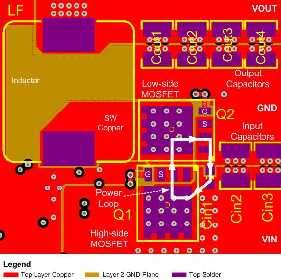
Figure 11-2 shows an example PCB layout based on the LM5145EVM-HD-20A design. The power component connections are made on the top layer with wide, copper-filled areas. A power ground plane is placed on layer 2 with 6 mil (0.15 mm) spacing to the top layer. The small area of the buck regulator hot loop is denoted by the white border in Figure 11-2. This is critical to minimize EMI as well as switch-node voltage overshoot and ringing.
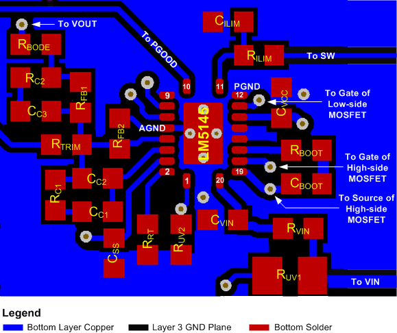
The LM5145 is located on the bottom side with a surrounding analog ground plane for sensitive analog components as shown in Figure 11-3. The analog ground plane (AGND) and power ground plane (PGND) are connected at a single point directly under the IC (at the die attach pad or DAP). Refer to the LM5145EVM-HD-20A High Density Evaluation Module User's Guide and LM5146-Q1-EVM12V Evaluation Module User's Guide for more detail.
 Figure 11-2 LM5145 Power Stage PCB Layout
 Figure 11-3 LM5145 Controller PCB Layout (Viewed From Top)