JAJSDA5B November 2017 – November 2020 LM5145
PRODUCTION DATA
- 1 特長
- 2 アプリケーション
- 3 概要
- 4 Revision History
- 5 Description (continued)
- 6 Pin Configuration and Functions
- 7 Specifications
-
8 Detailed Description
- 8.1 Overview
- 8.2 Functional Block Diagram
- 8.3
Feature Description
- 8.3.1 Input Range (VIN)
- 8.3.2 Output Voltage Setpoint and Accuracy (FB)
- 8.3.3 High-Voltage Bias Supply Regulator (VCC)
- 8.3.4 Precision Enable (EN/UVLO)
- 8.3.5 Power Good Monitor (PGOOD)
- 8.3.6 Switching Frequency (RT, SYNCIN)
- 8.3.7 Configurable Soft Start (SS/TRK)
- 8.3.8 Voltage-Mode Control (COMP)
- 8.3.9 Gate Drivers (LO, HO)
- 8.3.10 Current Sensing and Overcurrent Protection (ILIM)
- 8.3.11 OCP Duty Cycle Limiter
- 8.4 Device Functional Modes
-
9 Application and Implementation
- 9.1 Application Information
- 9.2
Typical Applications
- 9.2.1 Design 1 – 20-A High-Efficiency Synchronous Buck Regulator for Telecom Power Applications
- 9.2.2 Design 2 – High Density, 12-V, 10-A Rail With LDO Low-Noise Auxiliary Output for RF Power Applications
- 9.2.3 Design 3 – 150-W, Regulated 24-V Rail for Commercial Drone Applications With Output Voltage Tracking Feature
- 9.2.4 Design 4 – Powering a Multicore DSP From a 24-V or 48-V Rail
- 10Power Supply Recommendations
- 11Layout
- 12Device and Documentation Support
- 13Mechanical, Packaging, and Orderable Information
パッケージ・オプション
デバイスごとのパッケージ図は、PDF版データシートをご参照ください。
メカニカル・データ(パッケージ|ピン)
- RGY|20
サーマルパッド・メカニカル・データ
発注情報
8.3.5 Power Good Monitor (PGOOD)
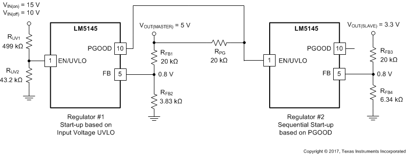
The LM5145 provides a PGOOD flag pin to indicate when the output voltage is within a regulation window. Use the PGOOD signal as shown in Figure 8-4 for start-up sequencing of downstream converters, fault protection, and output monitoring. PGOOD is an open-drain output that requires a pullup resistor to a DC supply not greater than 13 V. The typical range of pullup resistance is 10 kΩ to 100 kΩ. If necessary, use a resistor divider to decrease the voltage from a higher voltage pullup rail.
 Figure 8-4 Master-Slave Sequencing Implementation Using PGOOD and EN/UVLO
When the FB voltage exceeds 94% of the internal reference VREF, the internal PGOOD switch turns off and PGOOD can be pulled high by the external pullup. If the FB voltage falls below 92% of VREF, the internal PGOOD switch turns on, and PGOOD is pulled low to indicate that the output voltage is out of regulation. Similarly, when the FB voltage exceeds 108% of VREF, the internal PGOOD switch turns on, pulling PGOOD low. If the FB voltage subsequently falls below 105% of VREF, the PGOOD switch is turned off and PGOOD is pulled high. PGOOD has a built-in deglitch delay of 25 µs.