JAJSNZ8A February 2022 – April 2022 LM5152-Q1 , LM51521-Q1
PRODUCTION DATA
- 1 特長
- 2 アプリケーション
- 3 概要
- 4 Revision History
- 5 概要 (続き)
- 6 Device Comparison Table
- 7 Pin Configuration and Functions
- 8 Specifications
-
9 Detailed Description
- 9.1 Overview
- 9.2 Functional Block Diagram
- 9.3
Feature Description
- 9.3.1 Device Enable/Disable (EN, VH Pin)
- 9.3.2 High Voltage VCC Regulator (BIAS, VCC Pin)
- 9.3.3 Light Load Switching Mode Selection (MODE Pin)
- 9.3.4 Line Undervoltage Lockout (UVLO Pin)
- 9.3.5 Fast Restart Using VCC HOLD (VH Pin)
- 9.3.6 Adjustable Output Regulation Target (VOUT, TRK, VREF Pin)
- 9.3.7 Overvoltage Protection (VOUT Pin)
- 9.3.8 Boost Status Indicator (STATUS Pin)
- 9.3.9 Dynamically Programmable Switching Frequency (RT)
- 9.3.10 External Clock Synchronization (SYNC Pin)
- 9.3.11 Programmable Spread Spectrum (DITHER Pin)
- 9.3.12 Programmable Soft Start (SS Pin)
- 9.3.13 Wide Bandwidth Transconductance Error Amplifier and PWM (TRK, COMP Pin)
- 9.3.14 Current Sensing and Slope Compensation (CSP, CSN Pin)
- 9.3.15 Constant Peak Current Limit (CSP, CSN Pin)
- 9.3.16 Maximum Duty Cycle and Minimum Controllable On-Time Limits
- 9.3.17 Deep Sleep Mode and Bypass Operation (HO, CP Pin)
- 9.3.18 MOSFET Drivers, Integrated Boot Diode, and Hiccup Mode Fault Protection (LO, HO, HB Pin)
- 9.3.19 Thermal Shutdown Protection
- 9.4 Device Functional Modes
- 10Application and Implementation
- 11Power Supply Recommendations
- 12Layout
- 13Device and Documentation Support
- 14Mechanical, Packaging, and Orderable Information
パッケージ・オプション
メカニカル・データ(パッケージ|ピン)
- RGR|20
サーマルパッド・メカニカル・データ
- RGR|20
発注情報
9.3.17 Deep Sleep Mode and Bypass Operation (HO, CP Pin)
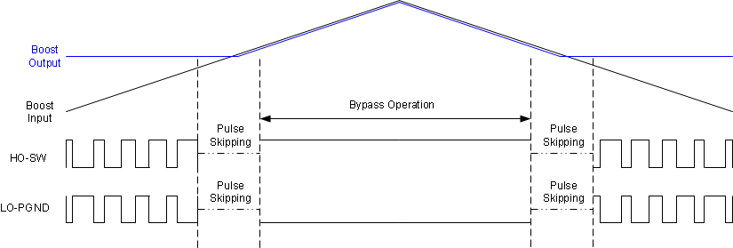
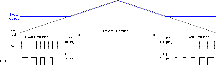
When SS is greater than 1.5 V, the device enters deep sleep mode after at least 40 μs in OVP status. The device re-enters active mode if VOUT falls down below VOVP. During bypass operation, the loss, which is caused by the body diode of the high-side MOSFET, is minimized. The high-side driver of the LM51521-Q1 does not turn on in the deep sleep mode. See Section 9.4.1.5 for more information.
 Figure 9-18 PWM to Bypass Transition in
CCM Operation
 Figure 9-19 PWM to Bypass Transition in
DCM Operation