JAJSNZ8A February 2022 – April 2022 LM5152-Q1 , LM51521-Q1
PRODUCTION DATA
- 1 特長
- 2 アプリケーション
- 3 概要
- 4 Revision History
- 5 概要 (続き)
- 6 Device Comparison Table
- 7 Pin Configuration and Functions
- 8 Specifications
-
9 Detailed Description
- 9.1 Overview
- 9.2 Functional Block Diagram
- 9.3
Feature Description
- 9.3.1 Device Enable/Disable (EN, VH Pin)
- 9.3.2 High Voltage VCC Regulator (BIAS, VCC Pin)
- 9.3.3 Light Load Switching Mode Selection (MODE Pin)
- 9.3.4 Line Undervoltage Lockout (UVLO Pin)
- 9.3.5 Fast Restart Using VCC HOLD (VH Pin)
- 9.3.6 Adjustable Output Regulation Target (VOUT, TRK, VREF Pin)
- 9.3.7 Overvoltage Protection (VOUT Pin)
- 9.3.8 Boost Status Indicator (STATUS Pin)
- 9.3.9 Dynamically Programmable Switching Frequency (RT)
- 9.3.10 External Clock Synchronization (SYNC Pin)
- 9.3.11 Programmable Spread Spectrum (DITHER Pin)
- 9.3.12 Programmable Soft Start (SS Pin)
- 9.3.13 Wide Bandwidth Transconductance Error Amplifier and PWM (TRK, COMP Pin)
- 9.3.14 Current Sensing and Slope Compensation (CSP, CSN Pin)
- 9.3.15 Constant Peak Current Limit (CSP, CSN Pin)
- 9.3.16 Maximum Duty Cycle and Minimum Controllable On-Time Limits
- 9.3.17 Deep Sleep Mode and Bypass Operation (HO, CP Pin)
- 9.3.18 MOSFET Drivers, Integrated Boot Diode, and Hiccup Mode Fault Protection (LO, HO, HB Pin)
- 9.3.19 Thermal Shutdown Protection
- 9.4 Device Functional Modes
- 10Application and Implementation
- 11Power Supply Recommendations
- 12Layout
- 13Device and Documentation Support
- 14Mechanical, Packaging, and Orderable Information
パッケージ・オプション
メカニカル・データ(パッケージ|ピン)
- RGR|20
サーマルパッド・メカニカル・データ
- RGR|20
発注情報
8.6 Typical Characteristics
Figure 8-1 Frequency vs RT Resistance
Figure 8-3 Frequency vs Temperature
(RT = 220 kΩ, 100 kHz)
(RT = 220 kΩ, 100 kHz)
Figure 8-5 VBIAS vs IBIAS (Bypass Mode, Charge Pump
On)
Figure 8-7 VBIAS vs IBIAS (Shutdown Mode)
Figure 8-9 VVCC vs IVCC
Figure 8-11 Peak
Current Limit Threshold vs VCSP
Figure 8-13 ICSP vs Temperature (Active Mode)
Figure 8-15 VOUT Sink Current vs Temperature (Deep Sleep)
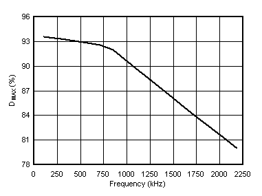
 Figure 8-17 DMAX vs
Frequency
Figure 8-17 DMAX vs
FrequencyFigure 8-2 Frequency vs Temperature
(RT = 9.09 kΩ, 2.2 MHz)
(RT = 9.09 kΩ, 2.2 MHz)
Figure 8-4 VBIAS vs IBIAS (Active Mode)
Figure 8-6 VBIAS vs IBIAS (Bypass Mode, Charge Pump
Off)
Figure 8-8 VBIAS vs VVCC
Figure 8-10 VVCC vs Peak
Driver Current
Figure 8-12 Peak
Current Limit Threshold VCLTH vs Temperature (CSP = 3 V)
Figure 8-14 VOUT
Sink Current vs VOUT (Deep Sleep)
Figure 8-16 VREF vs Temperature