JAJSG75B September 2018 – April 2024 LM5164-Q1
PRODUCTION DATA
- 1
- 1 特長
- 2 アプリケーション
- 3 概要
- 4 Pin Configuration and Functions
- 5 Specifications
-
6 Detailed Description
- 6.1 Overview
- 6.2 Functional Block Diagram
- 6.3
Feature Description
- 6.3.1 Control Architecture
- 6.3.2 Internal VCC Regulator and Bootstrap Capacitor
- 6.3.3 Regulation Comparator
- 6.3.4 Internal Soft Start
- 6.3.5 On-Time Generator
- 6.3.6 Current Limit
- 6.3.7 N-Channel Buck Switch and Driver
- 6.3.8 Synchronous Rectifier
- 6.3.9 Enable/Undervoltage Lockout (EN/UVLO)
- 6.3.10 Power Good (PGOOD)
- 6.3.11 Thermal Protection
- 6.4 Device Functional Modes
- 7 Application and Implementation
- 8 Device and Documentation Support
- 9 Revision History
- 10Mechanical, Packaging, and Orderable Information
パッケージ・オプション
メカニカル・データ(パッケージ|ピン)
- DDA|8
サーマルパッド・メカニカル・データ
- DDA|8
発注情報
5.6 Typical Characteristics
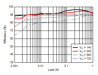 Figure 5-1 Conversion Efficiency (Log Scale)
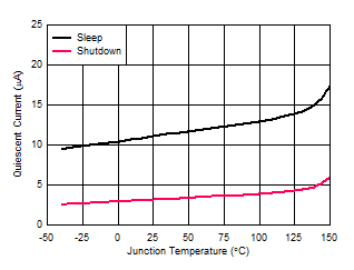 Figure 5-3 VIN Shutdown and Sleep Supply Current versus
Temperature
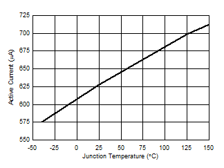 Figure 5-5 VIN Active Current versus Temperature
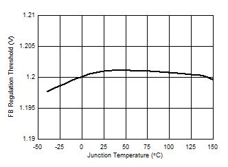 Figure 5-7 Feedback Comparator Threshold versus Temperature
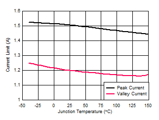 Figure 5-9 Peak
and Valley Current Limit versus Temperature
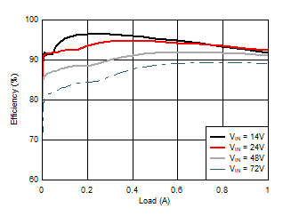 Figure 5-2 Conversion Efficiency (Linear Scale)
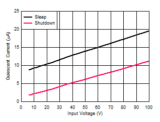 Figure 5-4 VIN Shutdown and Sleep Supply Current versus Input
Voltage
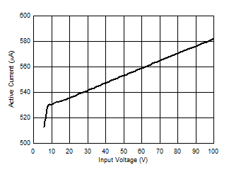 Figure 5-6 VIN Active Current versus Input Voltage
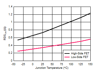 Figure 5-8 MOSFETs On-State Resistance versus Temperature
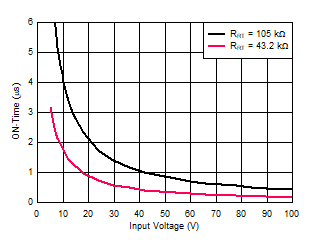 Figure 5-10 COT
On-Time versus VIN