SNVSCL2 December 2024 LM51770
PRODUCTION DATA
- 1
- 1 Features
- 2 Applications
- 3 Description
- 4 Device Comparison
- 5 Pin Configuration and Functions
- 6 Specifications
- 7 Parameter Measurement Information
-
8 Detailed Description
- 8.1 Overview
- 8.2 Functional Block Diagram
- 8.3
Feature Description
- 8.3.1 Power-On Reset (POR System)
- 8.3.2 Buck-Boost Control Scheme
- 8.3.3 Power Save Mode
- 8.3.4 Supply Voltage Selection – VMAX Switch
- 8.3.5 Enable and Undervoltage Lockout
- 8.3.6 Oscillator Frequency Selection
- 8.3.7 Frequency Synchronization
- 8.3.8 Voltage Regulation Loop
- 8.3.9 Output Voltage Tracking
- 8.3.10 Slope Compensation
- 8.3.11 Configurable Soft Start
- 8.3.12 Peak Current Sensor
- 8.3.13 Current Monitoring and Current Limit Control Loop
- 8.3.14 Short Circuit - Hiccup Protection
- 8.3.15 nFLT Pin and Protections
- 8.3.16 Device Configuration Pin
- 8.3.17 Dual Random Spread Spectrum – DRSS
- 8.3.18 Gate Driver
- 8.4 Device Functional Modes
-
9 Application and Implementation
- 9.1 Application Information
- 9.2
Typical Application
- 9.2.1
Detailed Design Procedure
- 9.2.1.1 Custom Design with WEBENCH Tools
- 9.2.1.2 Frequency
- 9.2.1.3 Feedback Divider
- 9.2.1.4 Inductor and Current Sense Resistor Selection
- 9.2.1.5 Slope Compensation
- 9.2.1.6 Output Capacitor
- 9.2.1.7 Input Capacitor
- 9.2.1.8 UVLO Divider
- 9.2.1.9 Soft-Start Capacitor
- 9.2.1.10 MOSFETs QH1 and QL1
- 9.2.1.11 MOSFETs QH2 and QL2
- 9.2.1.12 Frequency Compensation
- 9.2.1.13 External Component Selection
- 9.2.2 Application Curves
- 9.2.1
Detailed Design Procedure
- 10Power Supply Recommendations
- 11Layout
- 12Device and Documentation Support
- 13Revision History
- 14Mechanical, Packaging, and Orderable Information
8.3.7 Frequency Synchronization
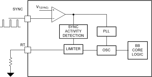
The device features an internal phase looked loop (PLL), which is designed to transition the switching frequency seamlessly between the frequency set by the RT pin and the external frequency synchronization signal. If no external frequency is provided, the RT pin sets the center frequency of the PLL. The external synchronization signal can change the switching frequency ±50%. To ensure low quiescence current, the input buffer of the SYNC pin is disabled if no valid sync frequency, that is a frequency signal outside the recommended synchronization range is applied.
If a valid synchronization frequency is applied, the device does not enter uSleep during the PSM pause. The internal PLL is kept active to quickly re-syncs to the external synchronization signal in case of a increased load e.g. due to a load step on the output. This behavior improves the transient responds but causes higher quiescent currents for light load operation because the uSleep is disabled if a synchronization signal is provide to the SYNC pin.
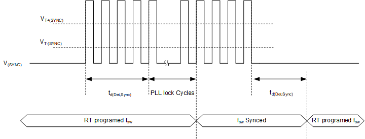
The synchronization timings are given in Figure 8-13.
 Figure 8-12 Main Oscillator Functional
Block Diagram
 Figure 8-13 Timing Diagram SYNC
Function
Figure 8-13 Timing Diagram SYNC
FunctionThe sync pin has a dual function to configure the current limit direction during the initialization phase. If pulled low during this time the negative current limit is selected. Otherwise the positive current limit is selected.