JAJSRX5 November 2023 LM5185
PRODUCTION DATA
- 1
- 1 特長
- 2 アプリケーション
- 3 概要
- 4 概要 (続き)
- 5 Pin Configuration and Functions
- 6 Specifications
-
7 Detailed Description
- 7.1 Overview
- 7.2 Functional Block Diagram
- 7.3
Feature Description
- 7.3.1 Power MOSFET Gate Driver
- 7.3.2 PSR Flyback Modes of Operation
- 7.3.3 High Voltage VCC Regulator
- 7.3.4 Setting the Output Voltage
- 7.3.5 Control Loop Error Amplifier
- 7.3.6 Precision Enable
- 7.3.7 Configurable Soft Start
- 7.3.8 Minimum On-Time and Off-Time
- 7.3.9 Current Sensing and Overcurrent Protection
- 7.3.10 Thermal Shutdown
- 7.4 Device Functional Modes
-
8 Application and Implementation
- 8.1 Application Information
- 8.2
Typical Applications
- 8.2.1
Design 1: Wide VIN, Low IQ PSR Flyback
Converter Rated at 16.4 V, 1 A
- 8.2.1.1 Design Requirements
- 8.2.1.2
Detailed Design Procedure
- 8.2.1.2.1 Custom Design With WEBENCH® Tools
- 8.2.1.2.2 Custom Design With Excel Quickstart Tool
- 8.2.1.2.3 Flyback Transformer T1 and Current-Sense Resistor (RCS)
- 8.2.1.2.4 Flyback Diode – DFLY
- 8.2.1.2.5 Leakage Inductance Clamp Circuit – DF, DCLAMP
- 8.2.1.2.6 Feedback Resistor – RFB
- 8.2.1.2.7 Thermal Compensation Resistor – RTC
- 8.2.1.2.8 UVLO Resistors – RUV1, RUV2
- 8.2.1.2.9 Soft-Start Capacitor – CSS
- 8.2.1.2.10 Compensation Components
- 8.2.1.3 Application Curves
- 8.2.1
Design 1: Wide VIN, Low IQ PSR Flyback
Converter Rated at 16.4 V, 1 A
- 8.3 Power Supply Recommendations
- 8.4 Layout
- 9 Device and Documentation Support
- 10Revision History
- 11Mechanical, Packaging, and Orderable Information
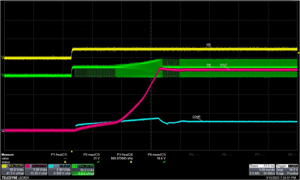
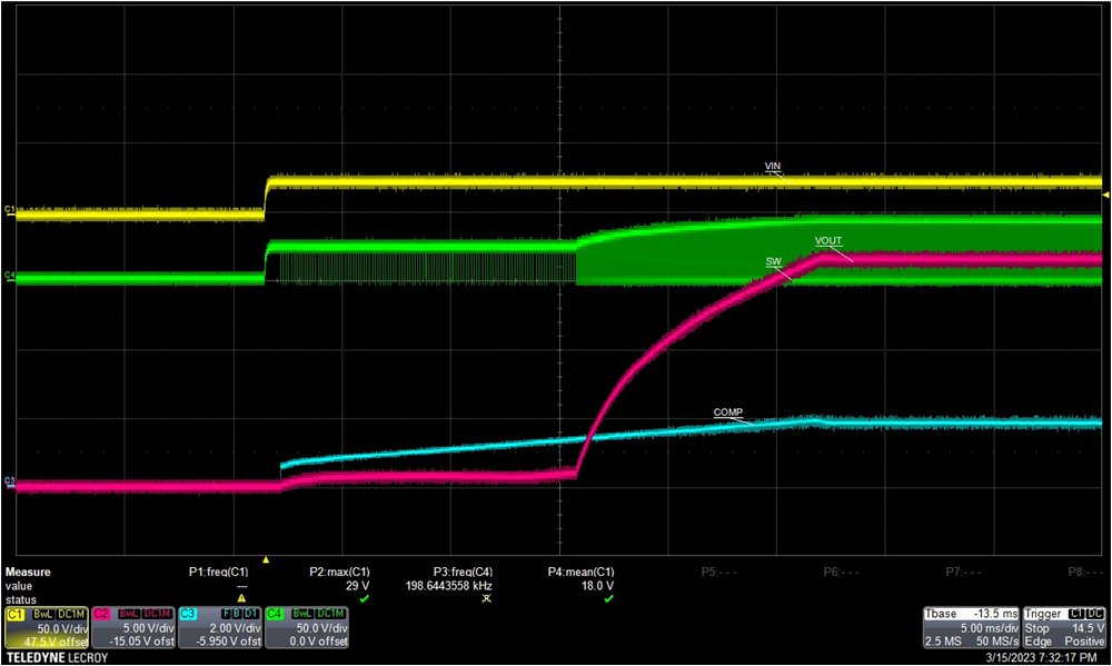
8.2.1.3 Application Curves
Unless otherwise stated, application performance curves were taken at TA = 25°C.


| VIN stepped to 24 V | 0-A Load | |


| VIN stepped to 24 V | 1-A Load | |