SNIS152E May 2009 – July 2015 LM57
PRODUCTION DATA.
- 1 Features
- 2 Applications
- 3 Description
- 4 Revision History
- 5 Device Comparison Table
- 6 Pin Configuration and Functions
-
7 Specifications
- 7.1 Absolute Maximum Ratings
- 7.2 ESD Ratings
- 7.3 Recommended Operating Conditions
- 7.4 Thermal Information
- 7.5 Electrical Characteristics - Accuracy Characteristics - Trip Point Accuracy
- 7.6 Electrical Characteristics - Accuracy Characteristics - VTEMP Analog Temperature Sensor Output Accuracy
- 7.7 Electrical Characteristics
- 7.8 Switching Characteristics
- 7.9 Typical Characteristics
-
8 Detailed Description
- 8.1 Overview
- 8.2 Functional Block Diagram
- 8.3 Feature Description
- 8.4 Device Functional Modes
- 9 Application and Implementation
- 10Power Supply Recommendations
- 11Layout
- 12Device and Documentation Support
- 13Mechanical, Packaging, and Orderable Information
パッケージ・オプション
メカニカル・データ(パッケージ|ピン)
サーマルパッド・メカニカル・データ
発注情報
9 Application and Implementation
NOTE
Information in the following applications sections is not part of the TI component specification, and TI does not warrant its accuracy or completeness. TI’s customers are responsible for determining suitability of components for their purposes. Customers should validate and test their design implementation to confirm system functionality.
9.1 Application Information
The LM57 has several outputs allowing for varying system implementations.
9.1.1 ADC Input Considerations
The LM57 has an analog temperature sensor output (VTEMP) that can be directly connected to an ADC (Analog to Digital Converter) input. Most CMOS ADCs found in microcontrollers and ASICs have a sampled data comparator input structure. When the ADC charges the sampling cap, it requires instantaneous charge from the output of the analog source such as the LM57 temperature sensor and many op amps. This requirement is easily accommodated by the addition of a capacitor (CFILTER). The size of CFILTER depends on the size of the sampling capacitor and the sampling frequency. Because not all ADCs have identical input stages, the charge requirements will vary. The general ADC application shown in Figure 20 is an example only.
 Figure 20. Suggested Connection to a Sampling Analog-to-Digital Converter Input Stage
9.2 Typical Application
 Figure 21. Typical Application Schematic with Microcontroller TRIP TEST Control
9.2.1 Design Requirements
By simply selecting the value of two resistors the trip point of the LM57 can easily be programmed as described in the following section. If standard 1% values are used the actual trip point threshold is not degraded and stands as described in the Electrical Characteristics section ().
9.2.2 Detailed Design Procedure
9.2.2.1 Selection of RSENSE Resistors
To set the trip point:
- Locate the desired trip temperature in Table 4.
- Identify the corresponding RSENSE2 value by following the column up to the resistor value.
- Identify the corresponding RSENSE1 value by following the row leftwards to the resistor value.
- Use only the EIA E96 standard resistor values from the list.
- Use only a resistor with 1% tolerance and a temperature coefficient of 100 ppm (or better). These restrictions are necessary to stay at the selected setting, and not to slip into an adjacent setting.
- This is consistent with using resistors from the thick film chip resistors CRCW0402 family. These are available with very small dimensions of L = 1 mm, W = 0.5 mm, H = 0.35 mm.
- Note that the resistor tolerance does not diminish the accuracy of the trip point. As can be seen in the block diagram these inputs drive the logic inputs of a DAC thus their tolerance does affect the trip point accuracy unless the DAC setting slips into an adjacent level. See patent number 6924758.
9.2.3 Application Curves
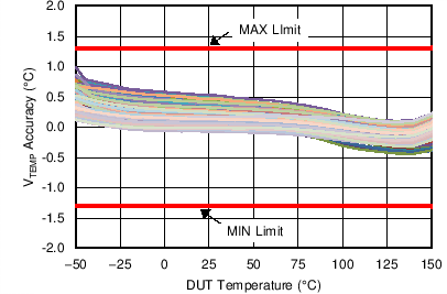
The typical performance of the LM57 temperature sensor output can be seen in Figure 22. Figure 23 shows the output behavior of the LM57 TOVER output.
 Figure 22. J2 VTEMP Accuracy Characteristics

9.2.4 Grounding of the TRIP TEST Pin
The circuit in Figure 24 shows the TRIP TEST pin grounded. This allows the LM57 to function autonomously without microcontroller intervention. In all other respects this circuit functions similarly to the circuit shown in Figure 21.
 Figure 24. Typical Application Schematic without Microcontroller TRIP TEST Control