JAJSIM1 February 2020 LM60430 , LM60440
ADVANCE INFORMATION for pre-production products; subject to change without notice.
- 1 特長
- 2 アプリケーション
- 3 概要
- 4 改訂履歴
- 5 Device Comparison Table
- 6 Pin Configuration and Functions
- 7 Specifications
- 8 Detailed Description
- 9 Application and Implementation
- 10Power Supply Recommendations
- 11Layout
- 12デバイスおよびドキュメントのサポート
- 13メカニカル、パッケージ、および注文情報
8.4.1 Auto Mode
In auto mode, the device moves between PWM and PFM as the load changes. At light loads, the regulator operates in PFM. At higher loads, the mode changes to PWM. The load current for which the device moves from PFM to PWM can be found in the Application Curves. The output current at which the device changes modes depends on the input voltage, inductor value, and the nominal switching frequency. For output currents above the curve, the device is in PWM mode. For currents below the curve, the device is in PFM. The curves apply for a nominal switching frequency of 400 kHz. At higher switching frequencies, the load at which the mode change occurs is greater. For applications where the switching frequency must be known for a given condition, the transition between PFM and PWM must be carefully tested before the design is finalized.
In PWM mode, the regulator operates as a constant frequency converter using PWM to regulate the output voltage. While operating in this mode, the output voltage is regulated by switching at a constant frequency and modulating the duty cycle to control the power to the load. This provides excellent line and load regulation and low output voltage ripple.
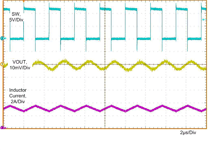
In PFM, the high-side MOSFET is turned on in a burst of one or more pulses to provide energy to the load. The duration of the burst depends on how long it takes the inductor current to reach IPEAK-MIN. The periodicity of these bursts is adjusted to regulate the output, while diode emulation (DEM) is used to maximize efficiency (see Glossary). This mode provides high light-load efficiency by reducing the amount of input supply current required to regulate the output voltage at light loads. PFM results in very good light-load efficiency, but also yields larger output voltage ripple and variable switching frequency. Also, a small increase in output voltage occurs at light loads. The actual switching frequency and output voltage ripple depends on the input voltage, output voltage, and load. Typical switching waveforms in PFM and PWM are shown in Figure 7 and Figure 8.
See the Application Curves for output voltage variation with load in auto mode.
 Figure 7. LM60430 Typical PFM Switching Waveforms
VIN = 12 V, VOUT = 5 V, IOUT = 10 mA
 Figure 8. LM60430 Typical PWM Switching Waveforms
VIN = 12 V, VOUT = 5 V, IOUT = 3 A, ƒS = 400 kHz