JAJSIM1 February 2020 LM60430 , LM60440
ADVANCE INFORMATION for pre-production products; subject to change without notice.
- 1 特長
- 2 アプリケーション
- 3 概要
- 4 改訂履歴
- 5 Device Comparison Table
- 6 Pin Configuration and Functions
- 7 Specifications
- 8 Detailed Description
- 9 Application and Implementation
- 10Power Supply Recommendations
- 11Layout
- 12デバイスおよびドキュメントのサポート
- 13メカニカル、パッケージ、および注文情報
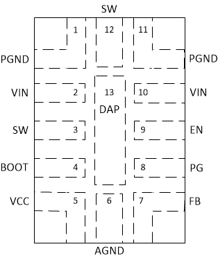
6 Pin Configuration and Functions
RPK Package
WQFN-13 With PowerPAD™
Top View

Pin Functions
| PIN | TYPE | DESCRIPTION | |
|---|---|---|---|
| NO. | NAME | ||
| 1, 11 | PGND | G | Power ground terminal. Connect to system ground and AGND. Connect to bypass capacitor with short wide traces. |
| 2, 10 | VIN | P | Input supply to regulator. Connect a high-quality bypass capacitor or capacitors directly to this pin and PGND. |
| 3, 12 | SW | P | Regulator switch node. Connect to power inductor. Pin 3 can be used to simplify the connection from the CBOOT capacitor to the SW pin. |
| 4 | BOOT | P | Bootstrap supply voltage for internal high-side driver. Connect a high-quality 100-nF capacitor from this pin to the SW pin. On the WQFN package, connect the SW pin to NC on the PCB. This simplifies the connection from the CBOOT capacitor to the SW pin. |
| 5 | VCC | P | Internal 5-V LDO output. Used as supply to internal control circuits. Do not connect to external loads. Can be used as logic supply for power-good flag. Connect a high quality 1-µF capacitor from this pin to GND. |
| 6 | AGND | G | Analog ground for regulator and system. Ground reference for internal references and logic. All electrical parameters are measured with respect to this pin. Connect to system ground on PCB. |
| 7 | FB | A | Feedback input to regulator. Connect to tap point of feedback voltage divider. Do not float. Do not ground. |
| 8 | PG | A | Open-drain power-good flag output. Connect to suitable voltage supply through a current limiting resistor. High = power OK, low = power bad. Flag pulls low when EN = Low. Can be left open when not used. |
| 9 | EN | A | Enable input to regulator. High = ON, low = OFF. Can be connected directly to VIN; Do not float. |
| 13 | DAP | — | Low impedance connection to PGND. Connect to system ground on PCB. Major heat dissipation path for the die. Must be used for heat sinking by soldering to ground copper on PCB. Thermal vias are preferred. |
| A = Analog, P = Power, G = Ground | |||