JAJSIQ7B March   2020  – June 2021 LM61435-Q1

PRODUCTION DATA  

  1. 特長
  2. アプリケーション
  3. 概要
  4. Revision History
  5. Device Comparison Table
  6. Pin Configuration and Functions
  7. Specifications
    1. 7.1 Absolute Maximum Ratings
    2. 7.2 ESD Ratings
    3. 7.3 Recommended Operating Conditions
    4. 7.4 Thermal Information
    5. 7.5 Electrical Characteristics
    6. 7.6 Timing Characteristics
    7. 7.7 Systems Characteristics
    8. 7.8 Typical Characteristics
  8. Detailed Description
    1. 8.1 Overview
    2. 8.2 Functional Block Diagram
    3. 8.3 Feature Description
      1. 8.3.1  EN/SYNC Uses for Enable and VIN UVLO
      2. 8.3.2  EN/SYNC Pin Uses for Synchronization
      3. 8.3.3  Clock Locking
      4. 8.3.4  Adjustable Switching Frequency
      5. 8.3.5  PGOOD Output Operation
      6. 8.3.6  Internal LDO, VCC UVLO, and BIAS Input
      7. 8.3.7  Bootstrap Voltage and VCBOOT-UVLO (CBOOT Pin)
      8. 8.3.8  Adjustable SW Node Slew Rate
      9. 8.3.9  Spread Spectrum
      10. 8.3.10 Soft Start and Recovery From Dropout
      11. 8.3.11 Output Voltage Setting
      12. 8.3.12 Overcurrent and Short Circuit Protection
      13. 8.3.13 Thermal Shutdown
      14. 8.3.14 Input Supply Current
    4. 8.4 Device Functional Modes
      1. 8.4.1 Shutdown Mode
      2. 8.4.2 Standby Mode
      3. 8.4.3 Active Mode
        1. 8.4.3.1 CCM Mode
        2. 8.4.3.2 Auto Mode - Light Load Operation
          1. 8.4.3.2.1 Diode Emulation
          2. 8.4.3.2.2 Frequency Reduction
        3. 8.4.3.3 FPWM Mode - Light Load Operation
        4. 8.4.3.4 Minimum On-time (High Input Voltage) Operation
        5. 8.4.3.5 Dropout
  9. Application and Implementation
    1. 9.1 Application Information
    2. 9.2 Typical Application
      1. 9.2.1 Design Requirements
      2. 9.2.2 Detailed Design Procedure
        1. 9.2.2.1  Choosing the Switching Frequency
        2. 9.2.2.2  Setting the Output Voltage
        3. 9.2.2.3  Inductor Selection
        4. 9.2.2.4  Output Capacitor Selection
        5. 9.2.2.5  Input Capacitor Selection
        6. 9.2.2.6  BOOT Capacitor
        7. 9.2.2.7  BOOT Resistor
        8. 9.2.2.8  VCC
        9. 9.2.2.9  BIAS
        10. 9.2.2.10 CFF and RFF Selection
        11. 9.2.2.11 External UVLO
      3. 9.2.3 Application Curves
  10. 10Power Supply Recommendations
  11. 11Layout
    1. 11.1 Layout Guidelines
      1. 11.1.1 Ground and Thermal Considerations
    2. 11.2 Layout Example
  12. 12Device and Documentation Support
    1. 12.1 Documentation Support
      1. 12.1.1 Related Documentation
    2. 12.2 Receiving Notification of Documentation Updates
    3. 12.3 サポート・リソース
    4. 12.4 Trademarks
    5. 12.5 Electrostatic Discharge Caution
    6. 12.6 Glossary
  13. 13Mechanical, Packaging, and Orderable Information

パッケージ・オプション

デバイスごとのパッケージ図は、PDF版データシートをご参照ください。

メカニカル・データ(パッケージ|ピン)
  • RJR|14
サーマルパッド・メカニカル・データ
発注情報

Application Curves

Unless otherwise specified, the following conditions apply: VIN = 13.5 V, TA = 25°C. The circuit is shown in , with the appropriate BOM from Table 9-5.
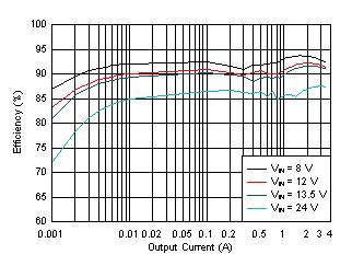
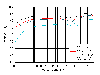
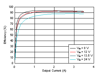
Unless otherwise specified, the following conditions apply: VIN = 13.5 V, TA = 25°C. The circuit is shown in , with the appropriate BOM from Table 9-5.GUID-E05437B5-C695-4D95-971B-9E9B2DF2C738-low.gif
VOUT = 3.3 V FSW = 2100 kHz AUTO Mode
Figure 9-5 LM61435-Q1 Efficiency. Unless otherwise specified, the following conditions apply: VIN = 13.5 V, TA = 25°C. The circuit is shown in , with the appropriate BOM from Table 9-5.
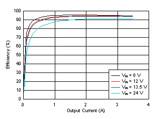
GUID-86746FB2-660B-4768-BA4C-863C3908981E-low.gif
VOUT = 5 V FSW = 2100 kHz AUTO Mode
Figure 9-7 LM61435-Q1 Efficiency
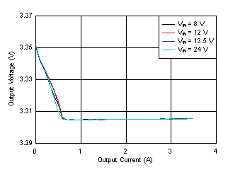
GUID-343F7A3C-53AF-4824-A29B-E06234A7274B-low.gif
VOUT = 3.3 V FSW = 400 kHz Auto Mode
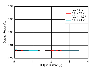
Figure 9-9 LM61435-Q1 Load and Line Regulation
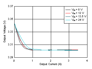
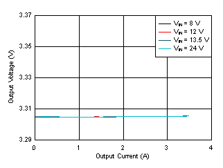
GUID-E786D271-2E3F-405C-9335-E43B2873A31F-low.gif
VOUT = 3.3 VFSW = 2100 kHzAuto Mode
Figure 9-11 LM61435-Q1 Load and Line Regulation
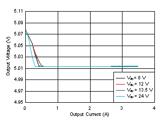
GUID-E17A68F8-5301-4B34-ADBA-766E788E5FB6-low.gif
VOUT = 5VFSW = 400 kHzAuto Mode
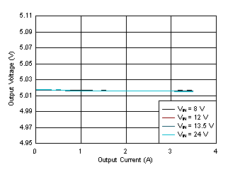
Figure 9-13 LM61435-Q1 Load and Line Regulation
GUID-E17A68F8-5301-4B34-ADBA-766E788E5FB6-low.gif
VOUT = 5VFSW = 2100 kHzAuto Mode
Figure 9-15 LM61435-Q1 Load and Line Regulation
GUID-F5FC89BE-CDE4-4E4E-ADAA-901274226A36-low.gif
VOUT = 3.3 VFSW = 400 kHzAUTO Mode
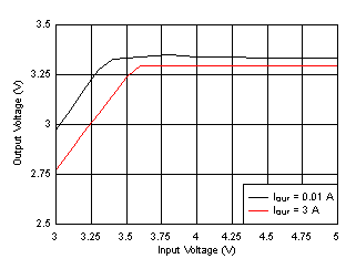
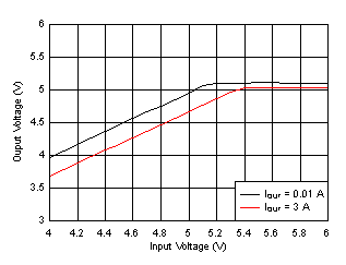
Figure 9-17 LM61435-Q1 Dropout Curve
GUID-8034D850-B774-4A9C-BF6E-745571038566-low.gif
VOUT = 5 VFSW = 400 kHzAUTO Mode
Figure 9-19 LM61435-Q1 Dropout Curve
GUID-C26407EB-4BFD-44D9-BFA5-97ECE49D5A4F-low.gif
VOUT = 3.3 VFSW = 400 kHzAUTO Mode
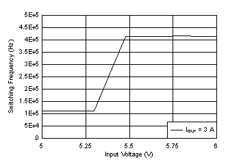
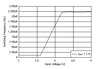
Figure 9-21 LM61435-Q1 Frequency Dropout Curve
GUID-540C72CE-05A4-4EFE-A1C5-29019D7C0A65-low.gif
VOUT = 5 V FSW = 400 kHz AUTO Mode
Figure 9-23 LM61435-Q1 Frequency Dropout Curve
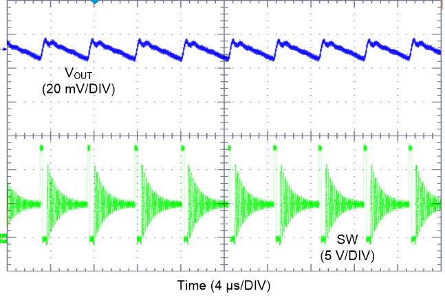
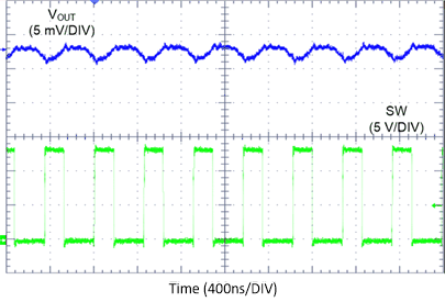
GUID-B9E3E8B9-3371-4692-A644-EE963C0EFBF1-low.png
VOUT = 5 V FSW = 2100 kHz AUTO Mode
IOUT = 100 mA VIN = 13.5 V
Figure 9-25 LM61435-Q1 Switching Waveform and VOUT Ripple
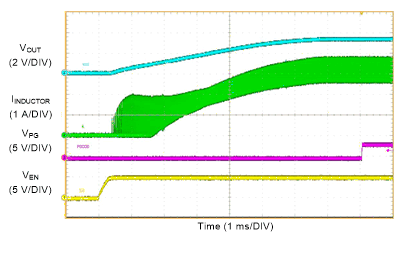
GUID-E0544198-D4D8-4969-818D-30B8BEACB74A-low.gif
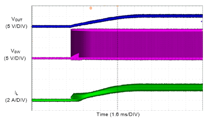
VOUT = 3.3 V FSW = 2100 kHz FPWM Mode
IOUT = 3.25 A VIN = 13.5 V
Figure 9-27 LM61435-Q1 Start-up with 3.25 A
GUID-BFD8501D-2F4F-4BC3-AEC6-80F758D5F8BE-low.gif
VOUT = 5 V FSW = 2100 kHz FPWM Mode
IOUT = Short Circuit to 2.5 A VIN = 13.5 V
Figure 9-29 LM61435-Q1 Short Circuit Recovery
GUID-8F701402-60C0-4E03-A6A5-5F5F382E8E2A-low.png
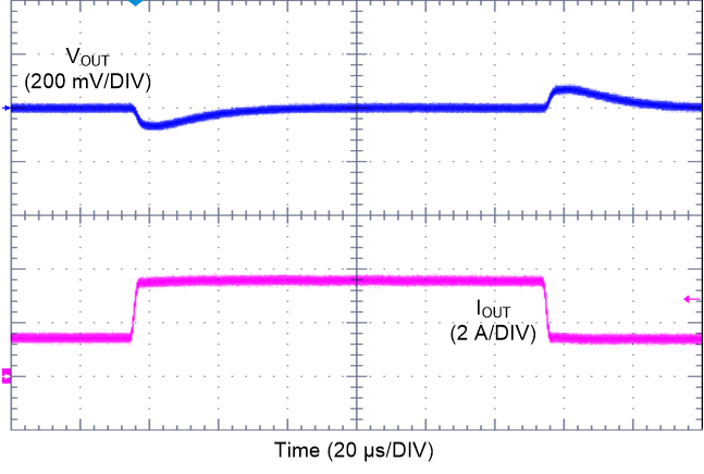
VOUT = 3.3 V FSW = 400 kHz AUTO Mode
IOUT = 1.5 A to 3.5 A to 1.5 A VIN = 13.5 V TR = TF = 2µs
Figure 9-31 LM61435-Q1 Load Transient
GUID-C701CEC3-4CB2-43EF-AD0F-6FFC76929742-low.png
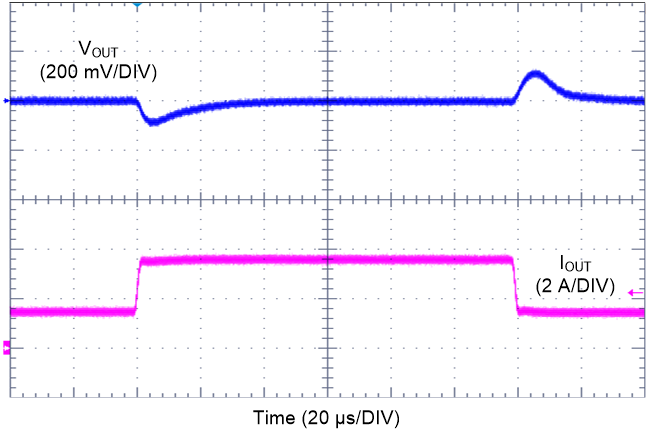
VOUT = 5 V FSW = 2100 kHz AUTO Mode
IOUT = 1.5 A to 3.5 A to 1.5 A VIN = 13.5 V TR = TF = 2µs
Figure 9-33 LM61435-Q1 Load Transient
GUID-709D350A-87B4-4502-8187-2686647F3667-low.gif
VOUT = 5 V FSW = 400 kHz IOUT = 5 A
Frequency Tested: 30 MHz to 108 MHz
Figure 9-35 Conducted EMI versus CISPR25 Limits (Yellow: Peak Signal, Blue: Average Signal)
GUID-7F9515A8-1E3C-4B95-8FFD-0A250C4CB0BC-low.gif
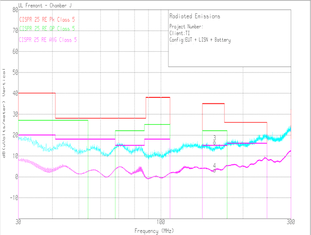
VOUT = 5 V FSW = 400 kHz IOUT = 5 A
Frequency Tested: 30 MHz to 300 MHz
Figure 9-37 Radiated EMI Bicon Vertical versus CISPR25 Limits
GUID-BCC037A1-9766-42BC-AC62-371D72391C22-low.gif
VOUT = 5 V FSW = 400 kHz IOUT = 5 A
Frequency Tested: 300 MHz to 1 GHz
Figure 9-39 Radiated EMI Log Vertical versus CISPR25 Limits
GUID-30368369-D87B-4A3E-AA1C-1A6DAAC6B3B3-low.gif


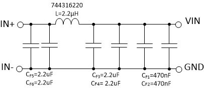
FSW = 400 kHzNote: Measurements taken with LM61460EVM with 6 A variant
Figure 9-41 Recommended Input EMI Filter
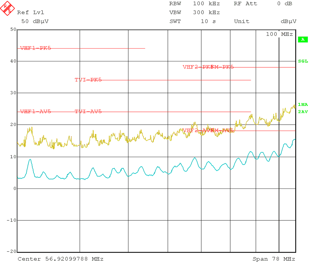
GUID-FCB87CD2-2895-459F-87E6-471B1212EB66-low.gif
FSW = 2100 kHzVOUT = 5 VIOUT = 5 A
Frequency Tested: 30 MHz to 108 MHz
Figure 9-43 Conducted EMI versus CISPR25 Limits (Yellow: Peak Signal, Blue: Average Signal)
GUID-739CA3E3-E4A4-453E-BD3F-8C6EA6D0C997-low.gif
VOUT = 3.3 V FSW = 2100 kHz FPWM Mode
Figure 9-6 LM61435-Q1 Efficiency
GUID-091A2C7E-2FC9-40F4-B90B-46D5415F7D47-low.gif
VOUT = 5 V FSW = 2100 kHz FPWM Mode
Figure 9-8 LM61435-Q1 Efficiency
GUID-17AD46C1-1ECC-4694-9698-066FEF0CAE23-low.gif
VOUT = 3.3 V FSW = 400 kHz FPWM Mode
Figure 9-10 LM61435-Q1 Load and Line Regulation
GUID-C38B382C-DE26-494E-A4B7-74BA10C5BE1F-low.gif
VOUT = 3.3 VFSW = 2100 kHzFPWM Mode
Figure 9-12 LM61435-Q1 Load and Line Regulation
GUID-56AA7242-28CA-4C80-90E8-A8FA17EBA0A7-low.gif
VOUT = 5 VFSW = 400 kHzFPWM Mode
Figure 9-14 LM61435-Q1 Load and Line Regulation
GUID-ED2C4F51-48F3-4F6E-870E-1BB64E78857B-low.gif
VOUT = 5VFSW = 2100 kHzFPWM Mode
Figure 9-16 LM61435-Q1 Load and Line Regulation
GUID-F128C873-7B06-49EA-99CC-1277DBC3037D-low.gif
VOUT = 3.3 VFSW = 2100 kHzAUTO Mode
Figure 9-18 LM61435-Q1 Dropout Curve
GUID-5DC76424-E923-4774-90AF-0F17E08C7632-low.gif
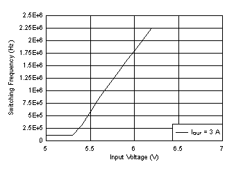
VOUT = 5 VFSW = 2100 kHzAUTO Mode
Figure 9-20 LM61435-Q1 Dropout Curve
GUID-BC81559A-4D84-4EB6-8F12-FEF5DC4587DB-low.gif
VOUT = 3.3 VFSW = 2100 kHzAUTO Mode
Figure 9-22 LM61435-Q1 Frequency Dropout Curve
GUID-61F97DFF-9A98-452D-95E0-9D23469591A2-low.gif
VOUT = 5 V FSW = 2100 kHz AUTO Mode
Figure 9-24 LM61435-Q1 Frequency Dropout Curve
GUID-0CE63BE0-1E05-4BBF-AF20-4021A5F0BCC4-low.gif
VOUT = 5 V FSW = 2100 kHz AUTO Mode
IOUT = 3.5 A VIN = 13.5 V
Figure 9-26 LM61435-Q1 Switching Waveform and VOUT Ripple
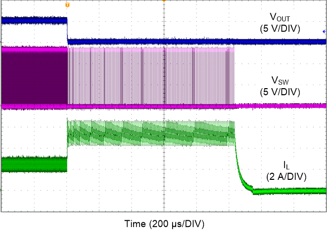
GUID-DCE5F40D-2F72-41A8-9E93-521DA218EAA4-low.png
VOUT = 5 V FSW = 2100 kHz FPWM Mode
IOUT = 2.5 A to Short Circuit VIN = 13.5 V
Figure 9-28 LM61435-Q1 Short Circuit Protection
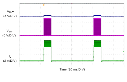
GUID-C43C5176-F0D7-4F58-851C-B872E21F59D0-low.gif
VOUT = 5 V FSW = 2100 kHz FPWM Mode
IOUT = Short Circuit VIN = 13.5 V
Figure 9-30 LM61435-Q1 Short Circuit Performance
GUID-6A9DB048-4882-4B1A-9457-104B3737B968-low.png
VOUT = 3.3 V FSW = 2100 kHz AUTO Mode
IOUT = 1.5 A to 3.5 A to 1.5 A VIN = 13.5 V TR = TF = 2µs
Figure 9-32 LM61435-Q1 Load Transient
GUID-1DD10277-E76E-40C0-9F76-AFA79D973493-low.gif
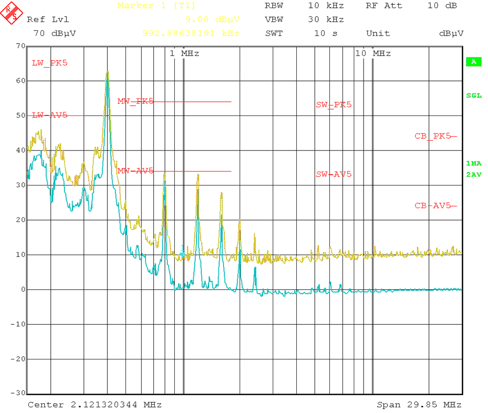
VOUT = 5 V FSW = 400 kHz IOUT = 5 A*
Frequency Tested: 150 kHz to 30 MHz
*Tested on 6 A Variant
Figure 9-34 Conducted EMI versus CISPR25 Limits (Yellow: Peak Signal, Blue: Average Signal)
GUID-00F8030D-043A-4144-9C16-F2CBC94751D9-low.gif
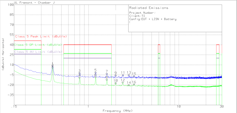
VOUT = 5 VFSW = 400 kHzIOUT = 5 A
Frequency Tested: 150 kHz to 30 MHz
Figure 9-36 Radiated EMI Rod versus CISPR25 Limits
GUID-7F9515A8-1E3C-4B95-8FFD-0A250C4CB0BC-low.gif
VOUT = 5 V FSW = 400 kHz IOUT = 5 A
Frequency Tested: 30 MHz to 300 MHz
Figure 9-38 Radiated EMI Bicon Horizontal versus CISPR25 Limits
GUID-4ED23289-EFBF-4BF8-B48D-DC0595234C06-low.gif
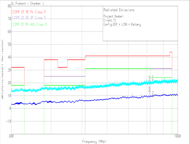
VOUT = 5 V FSW = 400 kHz IOUT = 5 A
Frequency Tested: 300 MHz to 1 GHz
Figure 9-40 Radiated EMI Log Horizontal versus CISPR25 Limits
GUID-CBE13FE3-EC6F-4458-B6B8-C5DF4CA4C093-low.gif
FSW = 2100 kHzVOUT = 5 VIOUT = 5 A*
Frequency Tested: 150 kHz to 30 MHz
*Tested on 6 A Variant
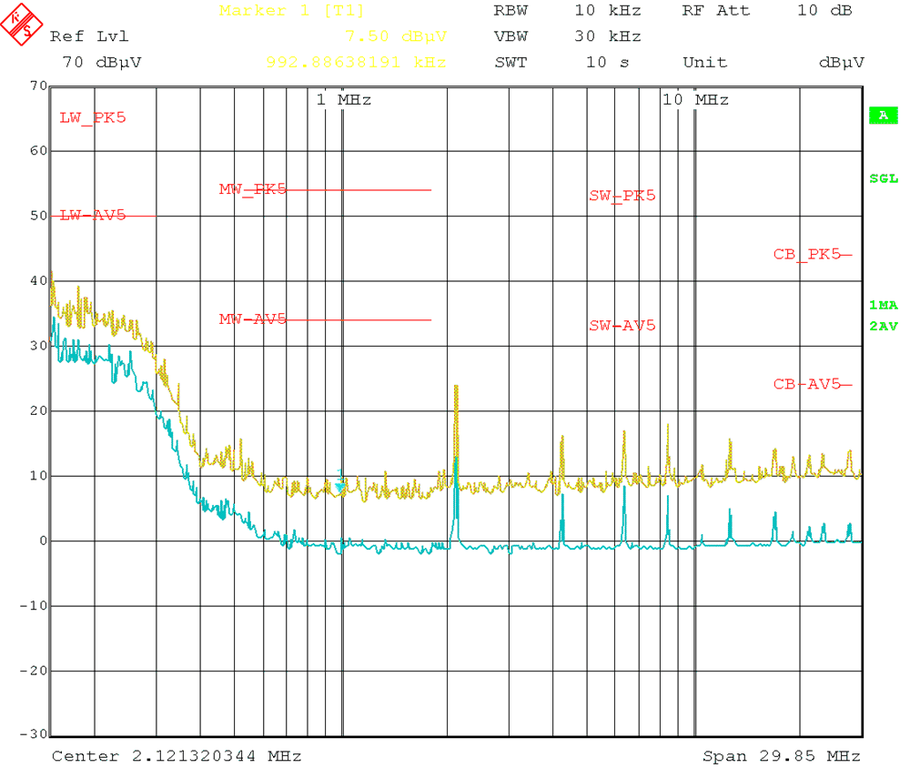
Figure 9-42 Conducted EMI versus CISPR25 Limits (Yellow: Peak Signal, Blue: Average Signal)
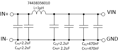
GUID-530F80E3-5A11-4730-885B-A04A81317BCE-low.gif


Note: All EMI measurements taken with 6 A Variant
FSW = 2100 kHz
Figure 9-44 Recommended Input EMI Filter
Table 9-5 BOM for Typical Application Curves
VOUTFREQUENCYRFBBRTCOUTCIN + CHFLCFF
3.3 V400 kHz43.2 kΩ33.2 kΩ4 x 22 µF2 x 4.7 µF + 2 x 100 nF8.2 µH (XHMI6060)22 pF
3.3 V2100 kHz43.2 kΩ6.04 kΩ3 x 22 µF2 x 4.7 µF + 2 x 100 nF1.5 µH (MAPI 4020HT)22 pF
5 V400 kHz24.9 kΩ33.2 kΩ3 x 22 µF2 x 4.7 µF + 2 x 100 nF8.2 µH (XHMI6060)22 pF
5 V2100 kHz24.9 kΩ6.04 kΩ2 x 22 µF2 x 4.7 µF + 2 x 100 nF1.5 µH (MAPI 4020HT)22 pF