SNVSCR9A October 2024 – December 2024 LM61480T-Q1 , LM61495T-Q1
PRODUCTION DATA
- 1
- 1 Features
- 2 Applications
- 3 Description
- 4 Device Comparison Table
- 5 Pin Configuration and Functions
- 6 Specifications
-
7 Detailed Description
- 7.1 Overview
- 7.2 Functional Block Diagram
- 7.3
Feature Description
- 7.3.1 Output Voltage Selection
- 7.3.2 Enable EN Pin and Use as VIN UVLO
- 7.3.3 SYNC/MODE Uses for Synchronization
- 7.3.4 Clock Locking
- 7.3.5 Adjustable Switching Frequency
- 7.3.6 RESET Output Operation
- 7.3.7 Internal LDO, VCC UVLO, and BIAS Input
- 7.3.8 Bootstrap Voltage and VCBOOT-UVLO (CBOOT Pin)
- 7.3.9 Adjustable SW Node Slew Rate
- 7.3.10 Spread Spectrum
- 7.3.11 Soft Start and Recovery From Dropout
- 7.3.12 Overcurrent and Short-Circuit Protection
- 7.3.13 Hiccup
- 7.3.14 Thermal Shutdown
- 7.4 Device Functional Modes
-
8 Application and Implementation
- 8.1 Application Information
- 8.2
Typical Application
- 8.2.1 Design Requirements
- 8.2.2
Detailed Design Procedure
- 8.2.2.1 Choosing the Switching Frequency
- 8.2.2.2 Setting the Output Voltage
- 8.2.2.3 Inductor Selection
- 8.2.2.4 Output Capacitor Selection
- 8.2.2.5 Input Capacitor Selection
- 8.2.2.6 BOOT Capacitor
- 8.2.2.7 BOOT Resistor
- 8.2.2.8 VCC
- 8.2.2.9 CFF and RFF Selection
- 8.2.2.10 RSPSP Selection
- 8.2.2.11 RT Selection
- 8.2.2.12 RMODE Selection
- 8.2.2.13 External UVLO
- 8.2.2.14 Maximum Ambient Temperature
- 8.2.3 Application Curves
- 8.3 Power Supply Recommendations
- 8.4 Layout
- 9 Device and Documentation Support
- 10Revision History
- 11Mechanical, Packaging, and Orderable Information
7.4.3.6 Recovery from Dropout
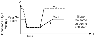
In some applications, input voltage can drop below the desired output voltage then recover to a higher value suddenly. With most regulators, the sudden increase in input voltage results in output voltage rising at a rate limited only by current limit until regulation is achieved. As input voltage reaches the desired output voltage, there is overshoot due to wind up in the control loop. This overshoot can be large in applications that have small output capacitors and light loads. Also, large inrush currents can cause large fluctuations on the input line after the regulator starts regulating the output voltage. This typically requires less current than during this initial inrush.
The LM614xxT-Q1 greatly reduces inrush current and overshoot. This reduction is done by engaging the soft-start circuit whenever the input voltage suddenly rises, after dipping low enough to cause the output voltage to droop. To prevent this feature from accidentally engaging, output voltage must fall more than 1% to engage this feature. Also, this feature engages only if operating in dropout or current limit, preventing interference with normal transient response but allowing several percent overshoot while engaging. If output voltage is very close to the desired level, overshoot is reduced by inductor current not having time to rise to a high level before regulation starts.
 Figure 7-26 When Output Voltage Falls, Output Voltage
Recovers Slowly Preventing Overshoot and Large Inrush Currents