JAJSJ65B May 2020 – June 2021 LM62435-Q1
PRODUCTION DATA
- 1 特長
- 2 アプリケーション
- 3 概要
- 4 Revision History
- 5 Device Comparison Table
- 6 Pin Configuration and Functions
- 7 Specifications
-
8 Detailed Description
- 8.1 Overview
- 8.2 Functional Block Diagram
- 8.3
Feature Description
- 8.3.1 EN Uses for Enable and VIN UVLO
- 8.3.2 MODE/SYNC Pin Operation
- 8.3.3 PGOOD Output Operation
- 8.3.4 Internal LDO, VCC UVLO, and BIAS Input
- 8.3.5 Bootstrap Voltage and VCBOOT-UVLO (CBOOT Pin)
- 8.3.6 Adjustable SW Node Slew Rate
- 8.3.7 Spread Spectrum
- 8.3.8 Soft Start and Recovery From Dropout
- 8.3.9 Output Voltage Setting
- 8.3.10 Overcurrent and Short Circuit Protection
- 8.3.11 Thermal Shutdown
- 8.3.12 Input Supply Current
- 8.4 Device Functional Modes
- 9 Application and Implementation
- 10Power Supply Recommendations
- 11Layout
- 12Device and Documentation Support
- 13Mechanical, Packaging, and Orderable Information
8.3.8 Soft Start and Recovery From Dropout
The LM62435-Q1 uses a reference-based soft start that prevents output voltage overshoots and large inrush currents during start-up. Soft start is triggered by any of the following conditions:
- Power is applied to the VIN pin of the IC, releasing UVLO.
- EN is used to turn on the device.
- Recovery from a hiccup waiting period
- Recovery from shutdown due to overtemperature protection
Once soft start is triggered, the IC takes the following actions:
- The reference used by the IC to regulate output voltage is slowly ramped. The net result is that output voltage takes tSS to reach 90% of its desired value.
- Operating mode is set to auto, activating diode emulation. This allows start-up without pulling output low if there is a voltage already present on output.
These actions together provide start-up with limited inrush currents and also allow the use of larger output capacitors and higher loading conditions that cause current to border on current limit during start-up without triggering hiccup. See Figure 8-15.

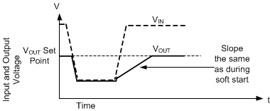
Any time the output voltage falls more than a few percent, the output voltage ramps up slowly. This condition is called recovery from dropout and differs from soft start in three important ways:
- The reference voltage is set to approximately 1% above what is needed to achieve the existing output voltage.
- Hiccup is allowed if output voltage is less than 0.4 times its set point. Note that during dropout regulation itself, hiccup is inhibited.
- FPWM mode is allowed during recovery from dropout. If the output voltage were to suddenly be pulled up by an external supply, the LM62435-Q1 can pull down on the output.
Despite being called recovery from dropout, this feature is active whenever output voltage drops to a few percent lower than the set point. This primarily occurs under the following conditions:
- Dropout: When there is insufficient input voltage for the desired output voltage to be generated
- Overcurrent: When there is an overcurrent event that is not severe enough to trigger hiccup
