JAJSJO6C December 2021 – August 2024 LM63440-Q1 , LM63460-Q1
PRODUCTION DATA
- 1
- 1 特長
- 2 アプリケーション
- 3 概要
- 4 Device Comparison Table
- 5 Pin Configuration and Functions
- 6 Specifications
-
7 Detailed Description
- 7.1 Overview
- 7.2 Functional Block Diagram
- 7.3
Feature Description
- 7.3.1 Input Voltage Range (VIN1, VIN2)
- 7.3.2 Output Voltage Setpoint (FB)
- 7.3.3 Precision Enable and Input Voltage UVLO (EN/SYNC)
- 7.3.4 Frequency Synchronization (EN/SYNC)
- 7.3.5 Clock Locking
- 7.3.6 Adjustable Switching Frequency (RT)
- 7.3.7 Power-Good Monitor (PGOOD)
- 7.3.8 Bias Supply Regulator (VCC, BIAS)
- 7.3.9 Bootstrap Voltage and UVLO (CBOOT)
- 7.3.10 Spread Spectrum
- 7.3.11 Soft Start and Recovery From Dropout
- 7.3.12 Overcurrent and Short-Circuit Protection
- 7.3.13 Thermal Shutdown
- 7.3.14 Input Supply Current
- 7.4 Device Functional Modes
-
8 Application and Implementation
- 8.1 Application Information
- 8.2
Typical Applications
- 8.2.1 Design 1 – Automotive Synchronous 6A Buck Regulator at 2.1MHz
- 8.2.2
Design 2 – Automotive Synchronous 4A Buck Regulator at 2.1MHz
- 8.2.2.1 Design Requirements
- 8.2.2.2
Detailed Design Procedure
- 8.2.2.2.1 Custom Design With WEBENCH® Tools
- 8.2.2.2.2 Setting the Output Voltage
- 8.2.2.2.3 Choosing the Switching Frequency
- 8.2.2.2.4 Inductor Selection
- 8.2.2.2.5 Output Capacitor Selection
- 8.2.2.2.6 Input Capacitor Selection
- 8.2.2.2.7 Bootstrap Capacitor
- 8.2.2.2.8 VCC Capacitor
- 8.2.2.2.9 BIAS Power Connection
- 8.2.2.2.10 Feedforward Network
- 8.2.2.2.11 Input Voltage UVLO
- 8.2.2.3 Application Curves
- 8.2.3 Design 3 – Automotive Synchronous 6A Buck Regulator at 400kHz
- 8.3 Power Supply Recommendations
- 8.4 Layout
- 9 Device and Documentation Support
- 10Revision History
- 11Mechanical, Packaging, and Orderable Information
8.2.2.2.6 Input Capacitor Selection
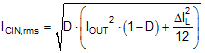
Input capacitors are necessary to limit the input ripple voltage of the converter due to switching-frequency AC currents. TI recommends using ceramic capacitors to provide low impedance and high RMS current rating over a wide temperature range. Equation 12 gives the input capacitor RMS current, where D = VOUT/VIN is the converter duty cycle. The highest input capacitor RMS current occurs at D = 0.5, at which point the RMS current rating of the capacitors must be greater than half the output current.
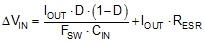
Ideally, the DC and AC components of input current to the buck stage are provided by the input voltage source and the input capacitors, respectively. Neglecting inductor ripple current, the input capacitors source current of amplitude (IOUT – IIN) during the D interval and sink IIN during the 1 – D interval. Thus, the input capacitors conduct a square-wave current of peak-to-peak amplitude equal to the output current. The resultant capacitive component of AC ripple voltage is a triangular waveform. Together with the ESR-related ripple component, Equation 13 gives the peak-to-peak ripple voltage amplitude:
Equation 14 gives the input capacitance required for a particular load current:
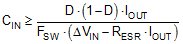
where
- ΔVIN is the input voltage ripple specification.
The Enhanced HotRod QFN package of the LM63440-Q1 and LM63460-Q1 provides two input voltage pins and two power ground pins on opposite sides of the package. This allows the input capacitors to be split and placed optimally with respect to the internal power MOSFETs, thus improving the effectiveness of the input bypassing. The converter requires a minimum of two 4.7µF ceramic input capacitors, preferably with X7R or X7S dielectric and in 1206 or 1210 footprint. In this example, place two 10μF, 50V ceramic capacitors in a symmetrical layout immediately adjacent to the converter – one at each input-to-ground pin pair: [VIN1, PGND1] and [VIN2, PGND2].
Install additional capacitance for automotive applications to meet conducted EMI specifications, such as CISPR 25 Class 5 (that limits EMI over a frequency range from 150kHz to 108MHz). For example, place a 10nF, 0402 ceramic capacitor at each input-to-ground pin pair immediately adjacent to the converter. These capacitors minimize the parasitic inductance in the switching loops and can suppress switch-node voltage overshoot and ringing, which reduces high-frequency EMI. The two 10nF capacitors, designated as CIN-HF1 and CIN-HF2 in Figure 8-1 or Figure 8-2, must be rated at 50V with an X7R or better dielectric.
As discussed in Section 8.3, a moderate-ESR electrolytic bulk capacitance (68µF to 100µF) at the input in parallel with the ceramics provides low-frequency filtering and parallel damping to mitigate the effects of input parasitic inductance resonating with the low-ESR, high-Q ceramic input capacitors. This is especially true if long leads or traces are used to connect the input supply to the converter.