JAJSJO6C December 2021 – August 2024 LM63440-Q1 , LM63460-Q1
PRODUCTION DATA
- 1
- 1 特長
- 2 アプリケーション
- 3 概要
- 4 Device Comparison Table
- 5 Pin Configuration and Functions
- 6 Specifications
-
7 Detailed Description
- 7.1 Overview
- 7.2 Functional Block Diagram
- 7.3
Feature Description
- 7.3.1 Input Voltage Range (VIN1, VIN2)
- 7.3.2 Output Voltage Setpoint (FB)
- 7.3.3 Precision Enable and Input Voltage UVLO (EN/SYNC)
- 7.3.4 Frequency Synchronization (EN/SYNC)
- 7.3.5 Clock Locking
- 7.3.6 Adjustable Switching Frequency (RT)
- 7.3.7 Power-Good Monitor (PGOOD)
- 7.3.8 Bias Supply Regulator (VCC, BIAS)
- 7.3.9 Bootstrap Voltage and UVLO (CBOOT)
- 7.3.10 Spread Spectrum
- 7.3.11 Soft Start and Recovery From Dropout
- 7.3.12 Overcurrent and Short-Circuit Protection
- 7.3.13 Thermal Shutdown
- 7.3.14 Input Supply Current
- 7.4 Device Functional Modes
-
8 Application and Implementation
- 8.1 Application Information
- 8.2
Typical Applications
- 8.2.1 Design 1 – Automotive Synchronous 6A Buck Regulator at 2.1MHz
- 8.2.2
Design 2 – Automotive Synchronous 4A Buck Regulator at 2.1MHz
- 8.2.2.1 Design Requirements
- 8.2.2.2
Detailed Design Procedure
- 8.2.2.2.1 Custom Design With WEBENCH® Tools
- 8.2.2.2.2 Setting the Output Voltage
- 8.2.2.2.3 Choosing the Switching Frequency
- 8.2.2.2.4 Inductor Selection
- 8.2.2.2.5 Output Capacitor Selection
- 8.2.2.2.6 Input Capacitor Selection
- 8.2.2.2.7 Bootstrap Capacitor
- 8.2.2.2.8 VCC Capacitor
- 8.2.2.2.9 BIAS Power Connection
- 8.2.2.2.10 Feedforward Network
- 8.2.2.2.11 Input Voltage UVLO
- 8.2.2.3 Application Curves
- 8.2.3 Design 3 – Automotive Synchronous 6A Buck Regulator at 400kHz
- 8.3 Power Supply Recommendations
- 8.4 Layout
- 9 Device and Documentation Support
- 10Revision History
- 11Mechanical, Packaging, and Orderable Information
7.3.11 Soft Start and Recovery From Dropout
The converter uses a reference-based soft start that prevents output voltage overshoot and large inrush current during start-up. Soft start is triggered by any of the following conditions:
- Power is applied to the VIN pins of the IC, releasing UVLO.
- EN/SYNC goes high to turn on the device.
- Recovery from a hiccup-waiting period
- Recovery from thermal shutdown protection
After soft start is triggered, the IC takes the following actions:
- The reference used by the IC to regulate the output voltage is slowly ramped. The net result is that the output voltage takes tSS to reach 90% of the desired value.
- The operating mode is set to AUTO, activating diode emulation. This action allows a pre-biased start-up without pulling the output voltage low if there is a voltage already present on the output.
Together, these actions provide start-up with limited inrush currents and also facilitate the use of high output capacitance and higher loading conditions that cause the peak inductor current to border on current limit during start-up without triggering hiccup. See Figure 7-6.

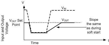
Any time the output voltage falls more than a few percent, the output voltage ramps up slowly. This condition is called recovery from dropout and differs from soft start in three important ways:
- The reference voltage is set to approximately 1% above what is needed to achieve the preset output voltage setpoint.
- Hiccup is allowed if the output voltage is less than 40% of the nominal setpoint. Note that during dropout regulation, hiccup is inhibited.
- FPWM mode is allowed during recovery from dropout. If the output voltage were to suddenly be pulled up by an external supply, the converter can pull down on the output.
Despite being called recovery from dropout, this feature is active whenever the output voltage drops to a few percent lower than the setpoint. This action primarily occurs under the following conditions:
- Dropout: When there is insufficient input voltage to maintain the desired output voltage
- Overcurrent: When there is an overcurrent event that is not severe enough to trigger hiccup
