JAJSF08G October 2017 – December 2020 LM74700-Q1
PRODMIX
- 1 特長
- 2 アプリケーション
- 3 概要
- 4 Revision History
- 5 Pin Configuration and Functions
- 6 Specifications
- 7 Typical Characteristics
- 8 Parameter Measurement Information
- 9 Detailed Description
-
10Application and Implementation
- 10.1 Application Information
- 10.2 OR-ing Application Configuration
- 11Power Supply Recommendations
- 12Layout
- 13Device and Documentation Support
- 14Mechanical, Packaging, and Orderable Information
パッケージ・オプション
メカニカル・データ(パッケージ|ピン)
サーマルパッド・メカニカル・データ
発注情報
10.1.1.3 Selection of TVS Diodes for 12-V Battery Protection Applications
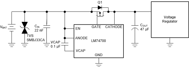
TVS diodes are used in automotive systems for protection against transients. In the 12-V battery protection application circuit shown in Figure 10-2, a bi-directional TVS diode is used to protect from positive and negative transient voltages that occur during normal operation of the car and these transient voltage levels and pulses are specified in ISO 7637-2 and ISO 16750-2 standards.
There are two important specifications are breakdown voltage and clamping voltage of the TVS. Breakdown voltage is the voltage at which the TVS diode goes into avalanche similar to a zener diode and is specified at a low current value typical 1 mA and the breakdown voltage should be higher than worst case steady state voltages seen in the system. The breakdown voltage of the TVS+ should be higher than 24-V jump start voltage and 35-V suppressed load dump voltage and less than the maximum ratings of LM74700-Q1 (65 V). The breakdown voltage of TVS- should be beyond than maximum reverse battery voltage –16 V, so that the TVS- is not damaged due to long time exposure to reverse connected battery.
Clamping voltage is the voltage the TVS diode clamps in high current pulse situations and this voltage is much higher than the breakdown voltage. TVS diodes are meant to clamp transient pulses and should not interfere with steady state operation. In the case of an ISO 7637-2 pulse 1, the input voltage goes up to –150 V with a generator impedance of 10 Ω. This translates to 15 A flowing through the TVS - and the voltage across the TVS would be close to its clamping voltage.
 Figure 10-2 Typical 12-V Battery Protection with Single
Bi-Directional TVS
Figure 10-2 Typical 12-V Battery Protection with Single
Bi-Directional TVSThe next criterion is that the absolute maximum rating of Anode to Cathode reverse voltage of the LM74700-Q1 (–75 V) and the maximum VDS rating MOSFET are not exceeded. In the design example, 60-V rated MOSFET is chosen and maximum limit on the cathode to anode voltage is 60 V.
In case of ISO 7637-2 pulse 1, the anode of LM74700-Q1 is pulled down by the ISO pulse and clamped by TVS-. The MOSFET is turned off quickly to prevent reverse current from discharging the bulk output capacitors. When the MOSFET turns off, the cathode to anode voltage seen is equal to (TVS Clamping voltage + Output capacitor voltage). If the maximum voltage on output capacitor is 16 V (maximum battery voltage), then the clamping voltage of the TVS- should not exceed, (60 V – 16) V = –44 V.
The SMBJ33CA TVS diode can be used for 12-V battery protection application. The breakdown voltage of 36.7 V meets the jump start, load dump requirements on the positive side and 16-V reverse battery connection on the negative side. During ISO 7637-2 pulse 1 test, the SMBJ33CA clamps at –44 V with 15 A of peak surge current as shown in Figure 10-5 and it meets the clamping voltage ≤ 44 V.
SMBJ series of TVS' are rated up to 600-W peak pulse power levels. This is sufficient for ISO 7637-2 pulses and suppressed load dump (ISO-16750-2 pulse B).