JAJSLG5 december 2022 LM7481
PRODUCTION DATA
- 1
- 1 特長
- 2 アプリケーション
- 3 概要
- 4 Revision History
- 5 Pin Configuration and Functions
- 6 Specifications
- 7 Parameter Measurement Information
- 8 Detailed Description
-
9 Application and Implementation
- 9.1 Application Information
- 9.2 Typical 12-V Reverse Battery Protection Application
- 9.3 Do's and Don'ts
- 9.4 Power Supply Recommendations
- 9.5 Layout
- 10Device and Documentation Support
- 11Mechanical, Packaging, and Orderable Information
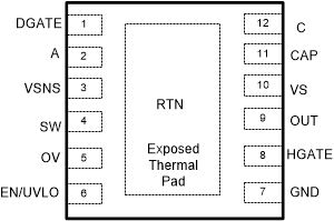
5 Pin Configuration and Functions
 Figure 5-1 DRR
Package, 12-Pin WSON(Top
View)
Figure 5-1 DRR
Package, 12-Pin WSON(Top
View)Table 5-1 Pin Functions
| PIN | TYPE(1) | DESCRIPTION | ||
|---|---|---|---|---|
| NAME | LM74810 | |||
| WSON | ||||
| DGATE | 1 | O | Diode Controller Gate Drive Output. Connect to the GATE of the external MOSFET. Anode of the ideal diode. | |
| A | 2 | I | Anode of the ideal diode. Connect to the source of the external MOSFET. | |
| VSNS | 3 | I | Voltage sensing input. | |
| SW | 4 | I | Voltage sensing disconnect switch terminal. VSNS and SW are internally connected through a switch. Use SW as the top connection of the battery sensing or OV resistor ladder network. When EN/UVLO is pulled low, the switch is OFF disconnecting the resistor ladder from the battery line thereby cutting off the leakage current. If the internal disconnect switch between VSNS and SW is not used then short them together and connect to VS pin. | |
| OV | 5 | I | Adjustable overvoltage threshold input. Connect a resistor ladder across SW to OV terminal. When the voltage at OVP exceeds the overvoltage cut-off threshold then the HGATE is pulled low turning OFF the HSFET. HGATE turns ON when the sense voltage goes below the OVP falling threshold. | |
| EN/UVLO | 6 | I | EN/UVLO Input. Connect to VS pin for always ON operation. Can be driven externally from a mirco controller I/O. Pulling it low below V(ENF) makes the device enter into low Iq shutdown mode. For UVLO, connect an external resistor ladder to EN/UVLO to GND. | |
| GND | 7 | G | Connect to the system ground plane. | |
| HGATE | 8 | O | GATE driver output for the HSFET. Connect to the GATE of the external FET. | |
| OUT | 9 | I | Connect to the output rail (external MOSFET source). | |
| VS | 10 | I | Input power supply to the IC. Connect VS to middle point of the common drain back to back MOSFET configuration. Connect a 100nF capacitor across VS and GND pins. | |
| CAP | 11 | O | Charge pump output. Connect a 100-nF capacitor across CAP and VS pins. | |
| C | 12 | I | Cathode of the ideal diode. Connect to the drain of the external MOSFET. | |
| RTN | Thermal Pad | — | Leave exposed pad floating. Do not connect to GND plane. | |
(1) I = input, O = output, I/O = input and output, P = power, G = Ground