JAJSOX6 October 2023 LM74930-Q1
PRODUCTION DATA
- 1
- 1 特長
- 2 アプリケーション
- 3 概要
- 4 Revision History
- 5 Pin Configuration and Functions
- 6 Specifications
-
7 Detailed Description
- 7.1 Overview
- 7.2 Functional Block Diagram
- 7.3
Feature Description
- 7.3.1 Charge Pump
- 7.3.2 Dual Gate Control (DGATE, HGATE)
- 7.3.3 Overcurrent Protection (CS+, CS-, ILIM, IMON, TMR)
- 7.3.4 Overcurrent Protection with Circuit Breaker (ILIM, TMR)
- 7.3.5 Overcurrent Protection With Latch-Off
- 7.3.6 Short-Circuit Protection (ISCP)
- 7.3.7 Analog Current Monitor Output (IMON)
- 7.3.8 Overvoltage and Undervoltage Protection (OV, UVLO, OVCLAMP)
- 7.3.9 Disabling Reverse Current Blocking Functionality (MODE)
- 7.3.10 Device Functional Modes
-
8 Applications and Implementation
- 8.1 Application Information
- 8.2
Typical Application: 200-V Unsuppressed Load Dump Protection Application
- 8.2.1 Design Requirements for 200-V Unsuppressed Load Dump Protection
- 8.2.2
Detailed Design Procedure
- 8.2.2.1 VS Capacitance, Resistor R1 and Zener Clamp (DZ)
- 8.2.2.2 Charge Pump Capacitance VCAP
- 8.2.2.3 Input and Output Capacitance
- 8.2.2.4 Overvoltage and Undervoltage Protection Component Selection
- 8.2.2.5 Selection of Scaling Resistor (RSET) and Short-Circuit Protection Setting Resistor (RSCP)
- 8.2.2.6 Overcurrent Limit (ILIM), Circuit Breaker Timer (TMR), and Current Monitoring Output (IMON) Selection
- 8.2.2.7 Selection of Current Sense Resistor, RSNS
- 8.2.2.8 Hold-Up Capacitance
- 8.2.2.9 MOSFET Q1 Selection
- 8.2.2.10 MOSFET Q2 Selection
- 8.2.2.11 Input TVS Selection
- 8.2.3 Application Curves
- 8.3 Best Design Practices
- 8.4 Power Supply Recommendations
- 8.5 Layout
- 9 Device and Documentation Support
- 10Mechanical, Packaging, and Orderable Information
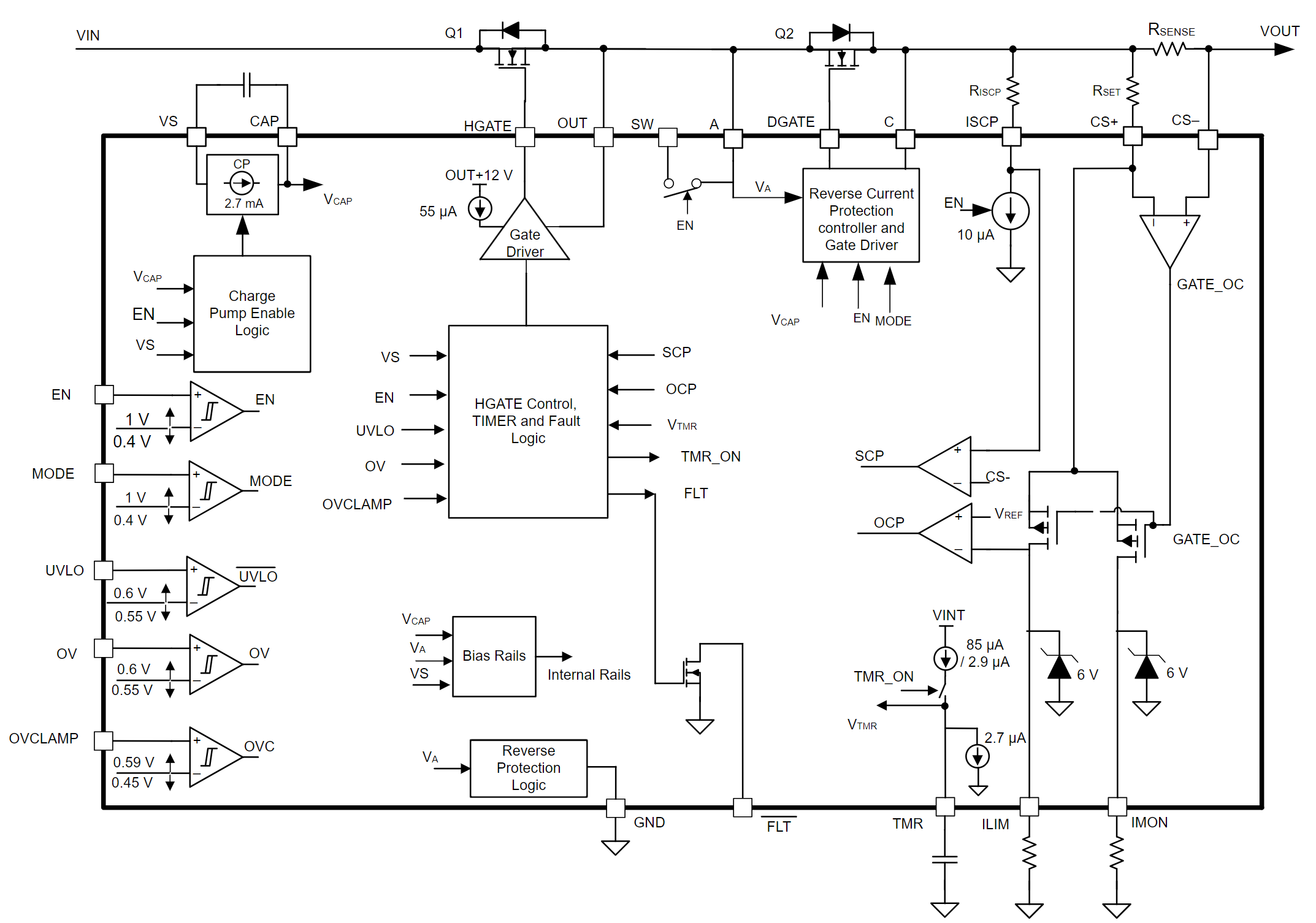
7.2 Functional Block Diagram
