JAJSAR0B March 2007 – October 2017 LM95214
PRODUCTION DATA.
- 1 特長
- 2 アプリケーション
- 3 概要
- 4 改訂履歴
- 5 概要(続き)
- 6 Pin Configuration and Functions
-
7 Specifications
- 7.1 Absolute Maximum Ratings
- 7.2 ESD Ratings
- 7.3 Recommended Operating Conditions
- 7.4 Thermal Information
- 7.5 Electrical Characteristics: Temperature-to-Digital Converter
- 7.6 Logic Electrical Characteristics: Digital DC Characteristics
- 7.7 Switching Characteristics: SMBus Digital
- 7.8 Typical Characteristics
-
8 Detailed Description
- 8.1 Overview
- 8.2 Functional Block Diagram
- 8.3 Feature Description
- 8.4 Device Functional Modes
- 8.5 Register Maps
- 9 Application and Implementation
- 10Power Supply Recommendations
- 11Layout
- 12デバイスおよびドキュメントのサポート
- 13メカニカル、パッケージ、および注文情報
8.4.2 Communicating With the LM95214
The data registers in the LM95214 are selected by the Command Register. At power-up the Command Register is set to 00, the location for the Read Local Temperature Register. The Command Register latches the last location it was set to. Each data register in the LM95214 falls into one of three types of user accessibility:
- Read only
- Write only
- Write/Read same address
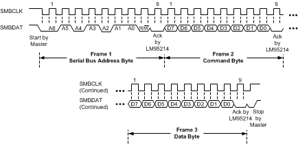
A Write to the LM95214 will always include the address byte and the command byte. A write to any register requires one data byte.
Reading the LM95214 can take place either of two ways:
- If the location latched in the Command Register is correct (most of the time it is expected that the Command Register will point to one of the Read Temperature Registers because that will be the data most frequently read from the LM95214), then the read can simply consist of an address byte, followed by retrieving the data byte.
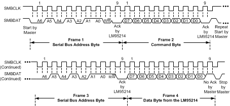
- If the Command Register needs to be set, then an address byte, command byte, repeat start, and another address byte will accomplish a read.
The data byte has the most significant bit first. At the end of a read, the LM95214 can accept either acknowledge or No Acknowledge from the Master (No Acknowledge is typically used as a signal for the slave that the Master has read its last byte). It takes the LM95214 190 ms (typical, all channels enabled) to measure the temperature of the remote diodes and internal diode. When retrieving all 11 bits from a previous remote diode temperature measurement, the master must insure that all 11 bits are from the same temperature conversion. This may be achieved by reading the MSB register first. The LSB will be locked after the MSB is read. The LSB will be unlocked after being read. If the user reads MSBs consecutively, each time the MSB is read, the LSB associated with that temperature will be locked in and override the previous LSB value locked-in.
 Figure 21. Serial Bus Write to the Internal Command Register Followed by a the Data Byte
 Figure 22. Serial Bus Write to the Internal Command Register
 Figure 23. Serial Bus Read From a Register With the Internal Command Register Preset to Desired Value
 Figure 24. Serial Bus Write Followed by a Repeat Start and Immediate Read