SNOS694I March 1995 – September 2015 LMC6001
PRODUCTION DATA.
- 1 Features
- 2 Applications
- 3 Description
- 4 Revision History
- 5 Pin Configuration and Functions
-
6 Specifications
- 6.1 Absolute Maximum Ratings
- 6.2 ESD Ratings
- 6.3 Recommended Operating Conditions
- 6.4 Thermal Information
- 6.5 DC Electrical Characteristics for LMC6001AI
- 6.6 DC Electrical Characteristics for LMC6001BI
- 6.7 DC Electrical Characteristics for LMC6001CI
- 6.8 AC Electrical Characteristics for LMC6001AIC
- 6.9 AC Electrical Characteristics for LM6001BI
- 6.10 AC Electrical Characteristics for LMC6001CI
- 6.11 Dissipation Ratings
- 6.12 Typical Characteristics
- 7 Detailed Description
- 8 Applications and Implementation
- 9 Power Supply Recommendations
- 10Layout
- 11Device and Documentation Support
- 12Mechanical, Packaging, and Orderable Information
1 Features
2 Applications
- Electrometer Amplifiers
- Photodiode Preamplifiers
- Ion Detectors
- A.T.E. Leakage Testing
3 Description
Featuring 100% tested input currents of 25 fA maximum, low operating power, and ESD protection of 2000 V, the LMC6001 device achieves a new industry benchmark for low input current operational amplifiers. By tightly controlling the molding compound, Texas Instruments is able to offer this ultra-low input current in a lower cost molded package.
To avoid long turnon settling times common in other low input current op amps, the LMC6001A is tested three times in the first minute of operation. Even units that meet the 25-fA limit are rejected if they drift.
Because of the ultra-low input current noise of 0.13 fA/√Hz, the LMC6001 can provide almost noiseless amplification of high resistance signal sources. Adding only 1 dB at 100 kΩ, 0.1 dB at 1 MΩ and 0.01 dB or less from 10 MΩ to 2,000 MΩ, the LMC6001 is an almost noiseless amplifier.
The LMC6001 is ideally suited for electrometer applications requiring ultra-low input leakage such as sensitive photodetection transimpedance amplifiers and sensor amplifiers. Because input referred noise is only 22 nV/√Hz, the LMC6001 can achieve higher signal to noise ratio than JFET input type electrometer amplifiers. Other applications of the LMC6001 include long interval integrators, ultra-high input impedance instrumentation amplifiers, and sensitive electrical-field measurement circuits.
Device Information(1)
| PART NUMBER | PACKAGE | BODY SIZE (NOM) |
|---|---|---|
| LMC6001 | PDIP (8) | 9.81 mm × 6.35 mm |
| TO-99 (8) | 9.08 mm × 9.08 mm |
- For all available packages, see the orderable addendum at the end of the data sheet.
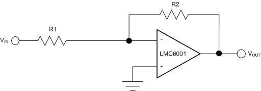
Simplified Schematic
