JAJS760E August 2000 – February 2024 LMC6081 , LMC6082 , LMC6084
PRODUCTION DATA
4 Pin Configuration and Functions
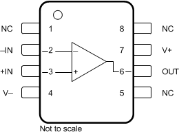
 Figure 4-1 LMC6081 D Package, 8-Pin SOIC, and P
Package, 8-Pin PDIP
Figure 4-1 LMC6081 D Package, 8-Pin SOIC, and P
Package, 8-Pin PDIPTable 4-1 Pin Functions: LMC6081
| PIN | TYPE(1) | DESCRIPTION | |
|---|---|---|---|
| NAME | NO. | ||
| +IN | 3 | Input | Noninverting input |
| –IN | 2 | Input | Inverting input |
| NC | 1, 5, 8 | — | No internal connection (can be left floating) |
| OUT | 6 | Output | Output |
| V+ | 7 | Power | Positive (highest) power supply |
| V– | 4 | Power | Negative (lowest) power supply |
 Figure 4-2 LMC6082 D Package, 8-Pin SOIC, and P Package, 8-Pin PDIP
Table 4-2 Pin Functions: LMC6081
| PIN | TYPE(1) | DESCRIPTION | |
|---|---|---|---|
| NAME | NO. | ||
| +IN A | 3 | Input | Noninverting input, channel A |
| –IN A | 2 | Input | Inverting input, channel A |
| +IN B | 5 | Input | Noninverting input, channel B |
| –IN B | 6 | Input | Inverting input, channel B |
| OUT A | 1 | Output | Output, channel A |
| OUT B | 7 | Output | Output, channel B |
| V+ | 8 | Power | Positive (highest) power supply |
| V– | 4 | Power | Negative (lowest) power supply |
 Figure 4-3 LMC6084 D Package, 8-Pin SOIC, and P Package, 8-Pin PDIP
Table 4-3 Pin Functions: LMC6084
| PIN | TYPE(1) | DESCRIPTION | |
|---|---|---|---|
| NAME | NO. | ||
| +IN A | 3 | Input | Noninverting input, channel A |
| +IN B | 5 | Input | Noninverting input, channel B |
| +IN C | 10 | Input | Noninverting input, channel C |
| +IN D | 12 | Input | Noninverting input, channel D |
| –IN A | 2 | Input | Inverting input, channel A |
| –IN B | 6 | Input | Inverting input, channel B |
| –IN C | 9 | Input | Inverting input, channel C |
| –IN D | 13 | Input | Inverting input, channel D |
| OUT A | 1 | Output | Output, channel A |
| OUT B | 7 | Output | Output, channel B |
| OUT C | 8 | Output | Output, channel C |
| OUT D | 14 | Output | Output, channel D |
| V+ | 4 | Power | Positive (highest) power supply |
| V– | 11 | Power | Negative (lowest) power supply |