JAJSD27B march 2017 – april 2023 LMG1205
PRODUCTION DATA
6.7 Typical Characteristics
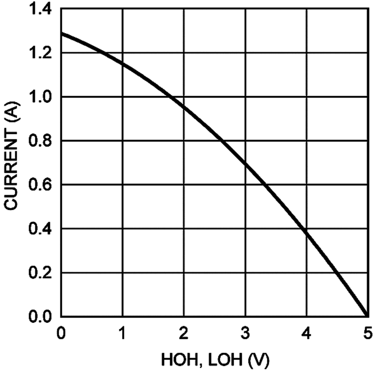 Figure 6-2 Peak Source Current vs Output Voltage
 Figure 6-4 IDDO vs Frequency
 Figure 6-6 IDD vs Temperature
 Figure 6-8 UVLO Rising Thresholds vs Temperature
 Figure 6-10 Input Thresholds vs Temperature
 Figure 6-12 Bootstrap Diode Forward Voltage
 Figure 6-14 LO & HO Gate Drive – High/Low Level Output Voltage vs Temperature
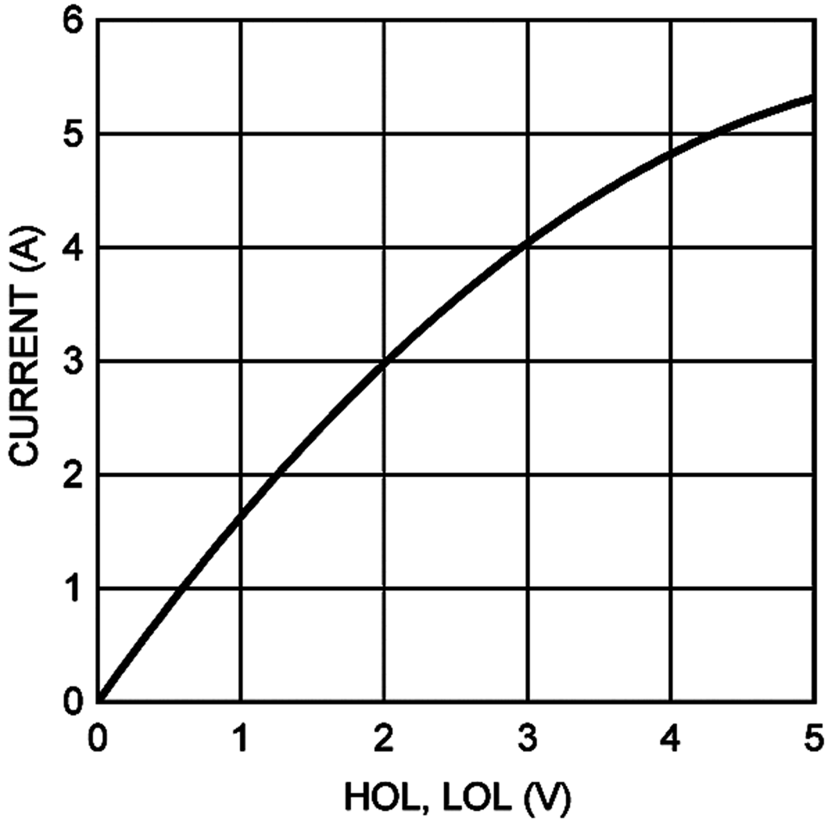 Figure 6-3 Peak Sink Current vs Output Voltage
 Figure 6-5 IHBO vs Frequency
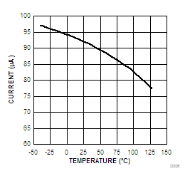 Figure 6-7 IHB vs Temperature
 Figure 6-9 UVLO Falling Thresholds vs Temperature
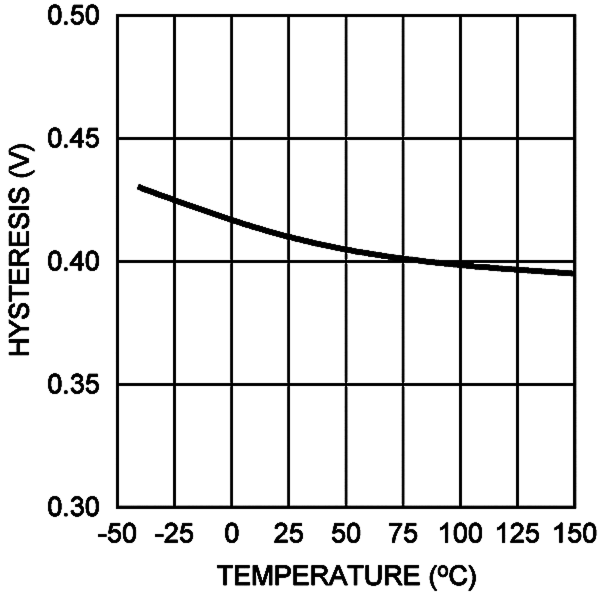 Figure 6-11 Input Threshold Hysteresis vs Temperature
 Figure 6-13 Propagation Delay vs Temperature
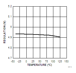 Figure 6-15 HB Regulation Voltage vs Temperature