JAJSD27B march 2017 – april 2023 LMG1205
PRODUCTION DATA
8.2.2.1 VDD Bypass Capacitor
The VDD bypass capacitor provides the gate charge for the low-side and high-side transistors and to absorb the reverse recovery charge of the bootstrap diode. The required bypass capacitance can be calculated with Equation 1.
Equation 1. 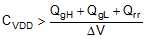
where
- QgH and QgL are gate charge of the high-side and low-side transistors, respectively
- Qrr is the reverse recovery charge of the bootstrap diode, which is typically around 4nC
- ΔV is the maximum allowable voltage drop across the bypass capacitor
TI recommends a 0.1–µF or larger value, good-quality ceramic capacitor. The bypass capacitor must be placed as close as possible to the device pins to minimize the parasitic inductance.