JAJSR52 September 2023 LMG3526R050
PRODUCTION DATA
- 1
- 1 特長
- 2 アプリケーション
- 3 概要
- 4 Revision History
- 5 Pin Configuration and Functions
- 6 Specifications
- 7 Parameter Measurement Information
-
8 Detailed Description
- 8.1 Overview
- 8.2 Functional Block Diagram
- 8.3
Feature Description
- 8.3.1 GaN FET Operation Definitions
- 8.3.2 Direct-Drive GaN Architecture
- 8.3.3 Drain-Source Voltage Capability
- 8.3.4 Internal Buck-Boost DC-DC Converter
- 8.3.5 VDD Bias Supply
- 8.3.6 Auxiliary LDO
- 8.3.7 Fault Detection
- 8.3.8 Drive-Strength Adjustment
- 8.3.9 Temperature-Sensing Output
- 8.3.10 Ideal-Diode Mode Operation
- 8.3.11 Zero-Voltage Detection (ZVD)
- 8.4 Start-Up Sequence
- 8.5 Safe Operation Area (SOA)
- 8.6 Device Functional Modes
- 9 Application and Implementation
- 10Device and Documentation Support
8.3.3 Drain-Source Voltage Capability
Due to the silicon FET’s long reign as the dominant power-switch technology, many designers are unaware that the headline drain-source voltage cannot be used as an equivalent point to compare devices across technologies. The headline drain-source voltage of a silicon FET is set by the avalanche breakdown voltage. The headline drain-source voltage of a GaN FET is set by the long term reliability with respect to data sheet specifications.
Exceeding the headline drain-source voltage of a silicon FET can lead to immediate and permanent damage. Meanwhile, the breakdown voltage of a GaN FET is much higher than the headline drain-source voltage. For example, the breakdown voltage of the LMG3526R050 is more than 800 V.
A silicon FET is usually the weakest link in a power application during an input voltage surge. Surge protection circuits must be carefully designed to ensure the silicon FET avalanche capability is not exceeded because it is not feasible to clamp the surge below the silicon FET breakdown voltage. Meanwhile, it is easy to clamp the surge voltage below a GaN FET breakdown voltage. In fact, a GaN FET can continue switching during the surge event which means output power is safe from interruption.
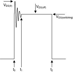
The LMG3526R050 drain-source capability is explained with the assistance of Figure 8-1. The figure shows the drain-source voltage versus time for a GaN FET for a single switch cycle in a switching application. No claim is made about the switching frequency or duty cycle.
 Figure 8-1 Drain-Source Voltage Switching
Cycle
Figure 8-1 Drain-Source Voltage Switching
CycleThe waveform starts before t0 with the FET in the on state. At t0 the GaN FET turns off and parasitic elements cause the drain-source voltage to ring at a high frequency. The peak ring voltage is designated VDS(tr). The high frequency ringing has damped out by t1. Between t1 and t2 the FET drain-source voltage is set by the characteristic response of the switching application. The characteristic is shown as a flat line, but other responses are possible. The voltage between t1 and t2 is designated VDS(off). At t2 the GaN FET is turned on at a non-zero drain-source voltage. The drain-source voltage at t2 is designated VDS(switching). Unique VDS(tr), VDS(off) and VDS(switching) parameters are shown because each can contribute to stress over the lifetime of the GaN FET.
The LMG3526R050 drain-source surge voltage capability is seen with the absolute maximum ratings VDS(tr)(surge) and VDS(surge) in the Specifications where VDS(tr)(surge) maps to VDS(tr) in Figure 8-1 and VDS(surge) maps to both VDS(off) and VDS(switching) in Figure 8-1. More information about the surge capability of TI GaN FETs is found in A New Approach to Validate GaN FET Reliability to Power-line Surges Under Use-conditions.