JAJSR52 September   2023 LMG3526R050

PRODUCTION DATA  

  1.   1
  2. 特長
  3. アプリケーション
  4. 概要
  5. Revision History
  6. Pin Configuration and Functions
  7. Specifications
    1. 6.1 Absolute Maximum Ratings
    2. 6.2 ESD Ratings
    3. 6.3 Recommended Operating Conditions
    4. 6.4 Thermal Information
    5. 6.5 Electrical Characteristics
    6. 6.6 Switching Characteristics
    7. 6.7 Typical Characteristics
  8. Parameter Measurement Information
    1. 7.1 Switching Parameters
      1. 7.1.1 Turn-On Times
      2. 7.1.2 Turn-Off Times
      3. 7.1.3 Drain-Source Turn-On Slew Rate
      4. 7.1.4 Zero-Voltage Detection Times
  9. Detailed Description
    1. 8.1 Overview
    2. 8.2 Functional Block Diagram
    3. 8.3 Feature Description
      1. 8.3.1  GaN FET Operation Definitions
      2. 8.3.2  Direct-Drive GaN Architecture
      3. 8.3.3  Drain-Source Voltage Capability
      4. 8.3.4  Internal Buck-Boost DC-DC Converter
      5. 8.3.5  VDD Bias Supply
      6. 8.3.6  Auxiliary LDO
      7. 8.3.7  Fault Detection
        1. 8.3.7.1 Overcurrent Protection and Short-Circuit Protection
        2. 8.3.7.2 Overtemperature Shutdown
        3. 8.3.7.3 UVLO Protection
        4. 8.3.7.4 Fault Reporting
      8. 8.3.8  Drive-Strength Adjustment
      9. 8.3.9  Temperature-Sensing Output
      10. 8.3.10 Ideal-Diode Mode Operation
        1. 8.3.10.1 Overtemperature-Shutdown Ideal-Diode Mode
      11. 8.3.11 Zero-Voltage Detection (ZVD)
    4. 8.4 Start-Up Sequence
    5. 8.5 Safe Operation Area (SOA)
      1. 8.5.1 Repetitive SOA
    6. 8.6 Device Functional Modes
  10. Application and Implementation
    1. 9.1 Application Information
    2. 9.2 Typical Application
      1. 9.2.1 Design Requirements
      2. 9.2.2 Detailed Design Procedure
        1. 9.2.2.1 Slew Rate Selection
          1. 9.2.2.1.1 Start-Up and Slew Rate With Bootstrap High-Side Supply
        2. 9.2.2.2 Signal Level-Shifting
        3. 9.2.2.3 Buck-Boost Converter Design
      3. 9.2.3 Application Curves
    3. 9.3 Do's and Don'ts
    4. 9.4 Power Supply Recommendations
      1. 9.4.1 Using an Isolated Power Supply
      2. 9.4.2 Using a Bootstrap Diode
        1. 9.4.2.1 Diode Selection
        2. 9.4.2.2 Managing the Bootstrap Voltage
    5. 9.5 Layout
      1. 9.5.1 Layout Guidelines
        1. 9.5.1.1 Solder-Joint Reliability
        2. 9.5.1.2 Power-Loop Inductance
        3. 9.5.1.3 Signal-Ground Connection
        4. 9.5.1.4 Bypass Capacitors
        5. 9.5.1.5 Switch-Node Capacitance
        6. 9.5.1.6 Signal Integrity
        7. 9.5.1.7 High-Voltage Spacing
        8. 9.5.1.8 Thermal Recommendations
      2. 9.5.2 Layout Examples
  11. 10Device and Documentation Support
    1. 10.1 Documentation Support
      1. 10.1.1 Related Documentation
    2. 10.2 ドキュメントの更新通知を受け取る方法
    3. 10.3 サポート・リソース
    4. 10.4 Trademarks
    5. 10.5 静電気放電に関する注意事項
    6. 10.6 Export Control Notice
    7. 10.7 用語集

パッケージ・オプション

メカニカル・データ(パッケージ|ピン)
サーマルパッド・メカニカル・データ
発注情報

Application Curves

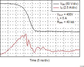
GUID-B3F4B4E4-B135-4C0F-9DBC-7E32E4A6D3E5-low.gifFigure 9-5 Turn-On Waveform in Application Example
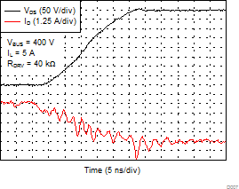
GUID-9FA7F1C6-1ED9-4016-8D2A-09937C2F53A4-low.gifFigure 9-6 Turn-Off Waveform in Application Example