SNLS270L August 2007 – January 2016 LMH0356
PRODUCTION DATA.
- 1 Features
- 2 Applications
- 3 Description
- 4 Revision History
- 5 Description (continued)
- 6 Pin Configuration and Functions
- 7 Specifications
- 8 Detailed Description
- 9 Application and Implementation
- 10Power Supply Recommendations
- 11Layout
- 12Device and Documentation Support
- 13Mechanical, Packaging, and Orderable Information
8 Detailed Description
8.1 Overview
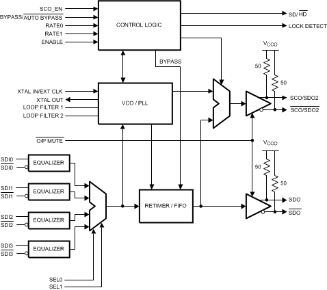
The LMH0356 3-Gbps HD/SD SDI Reclocker with 4:1 Input Mux and FR4 EQs is used in many types of digital video signal processing equipment. Supported serial digital video standards are ST-259, ST-292, and ST-424. Corresponding serial data rates are 270 Mbps, 1.483 Gbps, 1.485 Gbps, 2.967 Gbps, and 2.97 Gbps. DVB-ASI data at 270 Mbps may also be retimed. The LMH0356 retimes the serial data stream to suppress accumulated jitter. It provides two low-jitter, differential, serial data outputs. The second output may be selected to output either serial data or a low-jitter serial data-rate clock. Controls and indicators are: serial clock or second serial data output select, manual rate select input, SD/HD rate output, lock detect output, auto/manual data bypass and output mute.
Serial data inputs are CML and LVPECL compatible. Serial data and clock outputs are differential CML and produce LVPECL compatible levels. The output buffer design can drive AC or DC-coupled, terminated 100-Ω differential loads. The differential output level is 750 mVP-P into 100-Ω AC- or DC-coupled differential loads. Logic inputs and outputs are LVCMOS compatible.
The device package is a 48-pin WQFN or a 40-pin WQFN. Both package options have an exposed die attach pad. The exposed die attach pad is electrically connected to device ground (VEE) and is the primary electrical terminal for the device. This terminal must be connected to the negative power supply or circuit ground.
8.2 Functional Block Diagram

8.3 Feature Description
8.3.1 Functional Block Description
8.3.1.1 Serial Data Input and Outputs
The differential serial data inputs, SDI0-SDI3, accept serial digital video data at the rates specified in Table 1. Figure 2 shows the equivalent input circuit for SDI[3:0] and SDI[3:0]. The serial data inputs are differential LVPECL compatible. These inputs have 50-Ω internal terminations (100-Ω differential) with an internal bias as shown in Figure 2. These inputs are intended to be DC-coupled to devices such as the LMH0344 adaptive cable equalizer. DC-coupled inputs must be kept within the specified common mode range. The inputs may be AC-coupled if the input signal is outside the input common mode range of the device (such as when interfacing to 5-V PECL), and in that case the bias is supplied internally so no additional input biasing is required. See Figure 2 for more information on input interfacing.
The LMH0356 provides four independent, equalized and multiplexed data inputs. The active input channel is selected via the SEL0 and SEL1 pins, as shown in Table 2. The equalizer on each of the four inputs is capable of equalizing up to 30 inches of FR4 trace without the need for programming for different trace lengths or data rates.
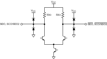
The LMH0356 has two retimed, differential, serial data outputs: SDO and SCO/SDO2. These outputs provide low-jitter, differential, retimed data to devices such as the LMH0302 cable driver. Output SCO/SDO2 is multiplexed and can provide either a second serial data output or a serial clock output. Figure 3 shows the equivalent output circuit for SDO, SDO, SCO/SDO2, and SCO/SDO2.
The SCO_EN input controls the operating mode for the SCO/SDO2 output. When the SCO_EN input is high the SCO/SDO2 output provides a serial clock. When SCO_EN is low, the SCO/SDO2 output provides retimed serial data.
Both differential serial data outputs, SDO and SCO/SDO2, are muted when the OUTPUT MUTE input is a logic low level. SCO/SDO2 also mutes when the Bypass mode is activated when this output is operating as the serial clock output. When muted, SDO and SDO (or SDO2 and SDO2) will assume opposite differential output levels. The CML serial data outputs are differential LVPECL compatible. These outputs have internal 50-Ω pullups and are suitable for driving AC- or DC-coupled, 100-Ω center-tapped, AC-grounded or 100-Ω un-center-tapped, differentially terminated networks.
![LMH0356 Equivalent SDI Input
Circuit (SDI[3:0], SDI[3:0]) LMH0356 30016708.gif](/ods/images/SNLS270L/30016708.gif) Figure 2. Equivalent SDI Input Circuit (SDI[3:0], SDI[3:0])
Figure 2. Equivalent SDI Input Circuit (SDI[3:0], SDI[3:0])
 Figure 3. Equivalent SDO Output Circuit (SDO, SDO, SCO/SDO2, SCO/SDO2)
8.3.1.2 Operating Serial Data Rates
This device operates at serial data rates of 270 Mbps, 1483 Mbps, 1485 Mbps, 2967 Mbps, and 2970 Mbps. The device does not lock to harmonics of these rates. The device does not lock and automatically enters the reclocker bypass mode for the following data rates: 143 Mbps, 177 Mbps, 360 Mbps, and 540 Mbps.
8.3.1.3 Serial Data Clock/Serial Data 2 Output
The Serial Data Clock/Serial Data 2 Output is controlled by the SCO_EN input and provides either a second retimed serial data output or a low jitter differential clock output appropriate to the serial data rate being processed. When operating as a serial clock output, the rising edge of the clock is positioned within the corresponding serial data bit interval within 10% of the center of the data interval.
Differential output SCO/SDO2 functions as the second serial data output when the SCO_EN input is a logic-low level. This output functions as the serial clock output when the SCO_EN input is a logic-high level. The SCO_EN input has an internal pulldown device and the default state of SCO_EN is low (serial data output 2 enabled). SCO/SDO2 is muted when the OUTPUT MUTE input is a logic low level. When the Bypass mode is activated and this output is functioning as a serial clock output, the output is muted. If an unsupported data rate is used while in Auto Bypass mode with this output functioning as a serial clock output, the output is invalid.
8.3.2 Control Inputs and Indicator Outputs
8.3.2.1 Serial Data Rate Selector
The Serial Data Rate Selector (RATE [1:0]) permits the user to fix the operating serial data rate. RATE[1:0] pins have internal pull-downs which maintain a logic-low input condition unless externally driven to a logic-high condition. This input also serves to place the device in a test mode. The codes shown in Table 1 select the desired operating serial data rate. The LMH0356 then enters either the Auto-Rate Detect mode or a single operating rate. Selecting the 270-Mbps rate mode may also be used when reclocking DVB-ASI data. DVB-ASI data is MPEG2 coded data that is transmitted in 8B10B coding. The device reclocks this data without harmonic locking.
Table 1. Data Rate Select Input Codes
| RATE [1:0] CODE |
DATA RATE OR MODE | COMMENTS |
|---|---|---|
| 00 | Auto-Rate Detect mode | |
| 01 | 270 Mbps | May be used to support DVB-ASI operation |
| 10 | 1483/1485 Mbps, 2967/2970 Mbps |
8.3.2.2 Serial Data Input Selector
The Serial Data Input Selector (SEL [1:0]) allows the user to select the active input channel. Table 2 shows the input selected for a given state of SEL [1:0]. The SEL pins have internal pulldowns.
Table 2. Data Input Select Codes
| SEL [1:0] CODE | SELECTED INPUT |
|---|---|
| 00 | SDI0 |
| 01 | SDI1 |
| 10 | SDI2 |
| 11 | SDI3 |
8.3.2.3 Lock Detect
The Lock Detect output, when high, indicates that data is being received and the PLL is locked. Lock Detect may be connected to the OUTPUT MUTE input to mute the data and clock outputs when no data signal is being received. Note that when the Bypass/Auto Bypass input is set high, Lock Detect will remain low. See Table 3.
8.3.2.4 OUTPUT MUTE
The OUTPUT MUTE input, when low, mutes the serial data and clock outputs. It may be connected to Lock Detect or externally driven to mute or un-mute the outputs. If OUTPUT MUTE is connected to Lock Detect, then the data and clock outputs are muted when the PLL is not locked. This function overrides the Bypass function; see Table 3. OUTPUT MUTE has an internal pullup device to enable the output by default.
8.3.2.5 Bypass/AUTO BYPASS
The Bypass/Auto Bypass input, when high, forces the device to output the data without reclocking it. When this input is low, the device automatically bypasses the reclocking function when the device is in an unlocked condition or the detected data rate is a rate which the device does not support. Note that when the Bypass/Auto Bypass input is set high, Lock Detect remains low. See Table 3. BYPASS/AUTO BYPASS has an internal pulldown device.
Table 3. Control Functionality
| LOCK DETECT | OUTPUT MUTE | BYPASS/AUTO BYPASS | DEVICE STATUS |
|---|---|---|---|
| 0 | 1 | X | PLL unlocked, reclocker bypassed |
| 1 | 1 | 0 | PLL locked to supported data rate, reclocker not bypassed |
| X | 0 | X | Outputs muted |
| 0 | LOCK DETECT | X | Outputs muted |
| 1 | LOCK DETECT | 0 | PLL locked to supported data rate, reclocker not bypassed |
8.3.2.6 SD/HD
The SD/HD output indicates whether the LMH0356 is processing SD or HD / 3 Gbps data rates. It may be used to control another device such as the LMH0302 cable driver. When this output is high it indicates that the data rate is 270 Mbps. When low, the indicated data rate is 1483, 1485, 2967, or 2970 Mbps. The SD/HD output is a registered function and is only valid when the PLL is locked and the Lock Detect output is high. When the PLL is not locked (the Lock Detect output is low), the SD/HD output defaults to HD (low). The SD/HD output is undefined for a short time after lock detect assertion or de-assertion due to a data rate change on SDI. See Figure 1 for a timing diagram showing the relationship between SDI, Lock Detect, and SD/HD.
8.3.2.7 SCO_EN
Input SCO_EN enables the SCO/SDO2 differential output to function either as a serial clock or second serial data output. SCO/SDO2 functions as a serial clock when SCO_EN is high. This pin has an internal pulldown device. The default state (low) enables the SCO/SDO2 output as a second serial data output.
8.3.2.8 ENABLE
The ENABLE pin is used to enable or disable the LMH0356. When the device is disabled, the output drivers and most of the internal circuitry are powered down. The crystal oscillator and external clock reference circuitry (XTAL IN and XTAL OUT) remain active regardless of the state of ENABLE, allowing the 27-MHz reference clock signal to be generated and passed on to additional reclockers. The ENABLE pin is active high and has an internal pullup device to enable the LMH0356 by default.
8.3.2.9 Crystal or External Clock Reference
The LMH0356 uses a 27-MHz crystal or external clock signal as a timing reference input. A 27-MHz parallel resonant crystal and load network may be connected to the XTAL IN/EXT CLK and XTAL OUT pins. Alternatively, a 27-MHz LVCMOS compatible clock signal may be input to XTAL IN/EXT CLK. Parameters for a suitable crystal are given in Table 4.
Table 4. Crystal Parameters
| PARAMETER | VALUE |
|---|---|
| Frequency | 27 MHz |
| Frequency stability | ±50 ppm at recommended drive level |
| Operating mode | Fundamental mode, parallel resonant |
| Load capacitance | 20 pF |
| Shunt capacitance | 7 pF |
| Series resistance | 40 Ω (maximum) |
| Recommended drive level | 100 µW |
| Maximum drive level | 500 µW |
| Operating temperature | −10°C to 60°C |
8.4 Device Functional Modes
The LMH0356 features are programmed using pin control. Refer to Control Inputs and Indicator Outputs for details.