SNLS315H April 2010 – August 2015 LMH0387
PRODUCTION DATA.
- 1 Features
- 2 Applications
- 3 Description
- 4 Revision History
- 5 Pin Configuration and Functions
-
6 Specifications
- 6.1 Absolute Maximum Ratings
- 6.2 ESD Ratings
- 6.3 Recommended Operating Conditions
- 6.4 Thermal Information
- 6.5 Control Pin Electrical Characteristics
- 6.6 Input Mode (Equalizer) DC Electrical Characteristics
- 6.7 Output Mode (Cable Driver) DC Electrical Characteristics
- 6.8 Input Mode (Equalizer) AC Electrical Characteristics
- 6.9 Output Mode (Cable Driver) AC Electrical Characteristics
- 6.10 Input Mode (Equalizer) SPI Interface AC Electrical Characteristics
- 6.11 Typical Characteristics
-
7 Detailed Description
- 7.1 Overview
- 7.2 Functional Block Diagram
- 7.3 Feature Description
- 7.4 Device Functional Modes
- 7.5 Programming
- 7.6 Register Maps
- 8 Application and Implementation
- 9 Power Supply Recommendations
- 10Layout
- 11Device and Documentation Support
- 12Mechanical, Packaging, and Orderable Information
8 Application and Implementation
NOTE
Information in the following applications sections is not part of the TI component specification, and TI does not warrant its accuracy or completeness. TI’s customers are responsible for determining suitability of components for their purposes. Customers should validate and test their design implementation to confirm system functionality.
8.1 Application Information
The LMH0387 is a single channel SDI cable driver and equalizer that supports different application spaces. The following sections describe the typical use cases and common implementation practices.
8.1.1 General Guidance for Applications
The LMH0387 supports SPI interface for configuring the device. Registers must be programmed (see Programming) for proper operation of the device. Attention must be paid to the PCB layout for the high speed signals to facilitate the SMPTE specification compliance. SMPTE specifies requirements for the Serial Digital Interface to transport digital video over coaxial cable. SMPTE specifies the use of AC coupling capacitors for transporting uncompressed serial data with heavy low-frequency content. This specification requires the use of a 4.7-μF AC coupling capacitor to avoid low-frequency DC wander. The 75-Ω trace impedance is required to meet SMPTE specified rise/fall requirements to facilitate highest eye opening for the receiving device.
8.2 Typical Application
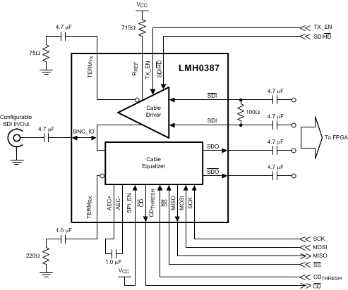
To meet SMPTE requirements, the optimal placement of the LMH0387 is to be as close to the BNC as possible. Figure 9 shows the application circuit for the LMH0387.
 Figure 9. Typical Application Schematic
8.2.1 Design Requirements
Table 2 lists the key design parameters of the LMH0387.
Table 2. Design Parameters
| DESIGN PARAMETER | REQUIREMENTS |
|---|---|
| Input AC coupling capacitor | Required. A common type of AC coupling capacitor is 4.7-µF ±10% X7R ceramic capacitor (0402 or 0201 size). |
| Trace or via under the device | No trace or via under the device. |
| Distance from device to BNC | Keep this distance as short as possible to minimize the parasitic. |
| BNC_IO, TERMTX, TERMRX trace impedance | Design single-ended trace impedance with 75 Ω ± 5%. |
| SDI, SDI and SDO, SDO differential trace impedance | Design differential trace impedance with 100 Ω ± 5%. |
| DC power supply coupling capacitors | To minimize power supply noise, use 0.1-µF shunt across 10-µF capacitors as close to the device as possible. |
8.2.2 Detailed Design Procedure
To begin the design process, determine the followings:
- Maximum power consumption for PCB regulator selection: Use maximum current consumption in the data sheet to compute the maximum power consumption.
- Closely compare schematic against typical connection diagram in the data sheet.
- With layout guideline in mind (see Layout Guidelines ) plan out the PCB layout and component placement to minimize parasitic.
- Consult the BNC vendor for optimum BNC landing pattern.
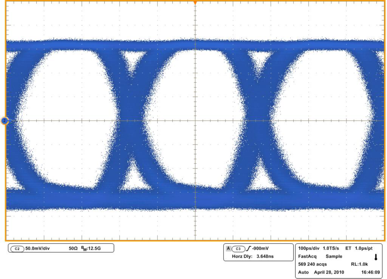
8.2.3 Application Curve
