SNLS315H April 2010 – August 2015 LMH0387
PRODUCTION DATA.
- 1 Features
- 2 Applications
- 3 Description
- 4 Revision History
- 5 Pin Configuration and Functions
-
6 Specifications
- 6.1 Absolute Maximum Ratings
- 6.2 ESD Ratings
- 6.3 Recommended Operating Conditions
- 6.4 Thermal Information
- 6.5 Control Pin Electrical Characteristics
- 6.6 Input Mode (Equalizer) DC Electrical Characteristics
- 6.7 Output Mode (Cable Driver) DC Electrical Characteristics
- 6.8 Input Mode (Equalizer) AC Electrical Characteristics
- 6.9 Output Mode (Cable Driver) AC Electrical Characteristics
- 6.10 Input Mode (Equalizer) SPI Interface AC Electrical Characteristics
- 6.11 Typical Characteristics
-
7 Detailed Description
- 7.1 Overview
- 7.2 Functional Block Diagram
- 7.3 Feature Description
- 7.4 Device Functional Modes
- 7.5 Programming
- 7.6 Register Maps
- 8 Application and Implementation
- 9 Power Supply Recommendations
- 10Layout
- 11Device and Documentation Support
- 12Mechanical, Packaging, and Orderable Information
6 Specifications
6.1 Absolute Maximum Ratings
over operating free-air temperature range (unless otherwise noted)(1)| MIN | MAX | UNIT | ||
|---|---|---|---|---|
| Supply Voltage | 4 | V | ||
| Input Voltage (all inputs) | −0.3 | VCC+0.3 | V | |
| Junction Temperature | 125 | °C | ||
| Storage Temperature | −65 | 150 | °C | |
(1) Stresses beyond those listed under Absolute Maximum Ratings may cause permanent damage to the device. These are stress ratings only, which do not imply functional operation of the device at these or any other conditions beyond those indicated under Recommended Operating Conditions. Exposure to absolute-maximum-rated conditions for extended periods may affect device reliability.
6.2 ESD Ratings
| VALUE | UNIT | |||
|---|---|---|---|---|
| V(ESD) | Electrostatic discharge | Human-body model (HBM), per ANSI/ESDA/JEDEC JS-001(1) | ±6000 | V |
| Charged-device model (CDM), per JEDEC specification JESD22-C101(2) | ±2500 | |||
| Machine model | ±300 | |||
(1) JEDEC document JEP155 states that 500-V HBM allows safe manufacturing with a standard ESD control process.
(2) JEDEC document JEP157 states that 250-V CDM allows safe manufacturing with a standard ESD control process.
6.3 Recommended Operating Conditions
| MIN | NOM | MAX | UNIT | |
|---|---|---|---|---|
| Supply Voltage (VCC – VEE) | 3.14 | 3.3 | 3.46 | V |
| BNC_IO Input / Output Coupling Capacitance | 4.7 | µF | ||
| AEC Capacitor (Connected between AEC+ and AEC-) | 1 | µF | ||
| Operating Free Air Temperature (TA) | −40 | 85 | °C |
6.4 Thermal Information
| THERMAL METRIC(1) | LMH0387 | UNIT | |
|---|---|---|---|
| NPD (TLGA) | |||
| 48 PINS | |||
| RθJA | Junction-to-ambient thermal resistance | 64.5 | °C/W |
| RθJC(top) | Junction-to-case (top) thermal resistance | 20.8 | °C/W |
| RθJB | Junction-to-board thermal resistance | 32.3 | °C/W |
| ψJT | Junction-to-top characterization parameter | 0.9 | °C/W |
| ψJB | Junction-to-board characterization parameter | 32 | °C/W |
| RθJC(bot) | Junction-to-case (bottom) thermal resistance | N/A | °C/W |
(1) For more information about traditional and new thermal metrics, see the Semiconductor and IC Package Thermal Metrics application report, SPRA953.
6.5 Control Pin Electrical Characteristics
Over Supply Voltage and Operating Temperature ranges, unless otherwise specified(1)(2).| PARAMETER | TEST CONDITIONS | MIN | TYP | MAX | UNIT | |
|---|---|---|---|---|---|---|
| VIH | Input Voltage High Level | 2 | VCC | V | ||
| VIL | Input Voltage Low Level | VEE | 0.8 | V | ||
| VOH | Output Voltage High Level | IOH = –2 mA | 2.4 | V | ||
| VOL | Output Voltage Low Level | IOL = 2 mA | 0.4 | V | ||
6.6 Input Mode (Equalizer) DC Electrical Characteristics
Over Supply Voltage and Operating Temperature ranges, unless otherwise specified(1)(2).| PARAMETER | TEST CONDITIONS | MIN | TYP | MAX | UNIT | |
|---|---|---|---|---|---|---|
| VIN | Input Voltage Swing | 0-m cable length(4) | 720 | 800 | 950 | mVP−P |
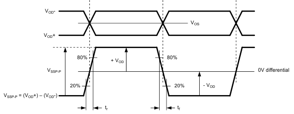
| VSSP-P | Differential Output Voltage, P-P | 100-Ω load, default register settings, Figure 1(5) | 500 | 700 | 900 | mVP-P |
| VOD | Differential Output Voltage | 250 | 350 | 450 | mV | |
| ΔVOD | Change in Magnitude of VOD for complementary Output States | 50 | mV | |||
| VOS | Offset Voltage | 1.125 | 1.25 | 1.375 | V | |
| ΔVOS | Change in Magnitude of VOS for complementary Output States | 50 | mV | |||
| IOS | Output Short Circuit Current | 30 | mA | |||
| CDTHRESH | CDTHRESH DC Voltage (floating) | 1.3 | V | |||
| CDTHRNG | CDTHRESH Range | 0.8 | V | |||
| ICC | Supply Current | Equalizing cable > 120 m (Belden 1694A), TX_EN = 0 |
91 | 113 | mA | |
| Equalizing cable ≤ 120 m (Belden 1694A), TX_EN = 0(6) |
71 | mA | ||||
| Power save mode (equalizer in sleep mode, TX_EN = 0) | 11 | mA | ||||
6.7 Output Mode (Cable Driver) DC Electrical Characteristics
Over Supply Voltage and Operating Temperature ranges, unless otherwise specified(1)(2).| PARAMETER | TEST CONDITIONS | MIN | TYP | MAX | UNIT | |
|---|---|---|---|---|---|---|
| VCMOUT | BNC_IO Output Common Mode Voltage | VCC – VOUT | V | |||
| VOUT | BNC_IO Output Voltage Swing | RREF = 715 Ω ±1% | 720 | 800 | 880 | mVP-P |
| VCMIN | SDI, SDI Input Common Mode Voltage | 0.9 + VID/2 | VCC – VID/2 | V | ||
| VID | SDI, SDI Input Voltage Swing | Differential | 100 | 2200 | mVP-P | |
| ICC | Supply Current | SD/HD = 0, equalizer in sleep mode | 57 | 71 | mA | |
| SD/HD = 1, equalizer in sleep mode | 50 | mA | ||||
| Power save mode (TX_EN = 0, equalizer in sleep mode) | 11 | mA | ||||
| Loopback mode (Tx and Rx both enabled), SD/HD = 0 | 117 | mA | ||||
6.8 Input Mode (Equalizer) AC Electrical Characteristics
Over Supply Voltage and Operating Temperature ranges, unless otherwise specified(2).| PARAMETER | TEST CONDITIONS | MIN | TYP | MAX | UNIT | |
|---|---|---|---|---|---|---|
| DRMIN | Minimum Input Data Rate | 125 | Mbps | |||
| DRMAX | Maximum Input Data Rate | 2970 | Mbps | |||
| tjit | Equalizer Jitter for Various Cable Lengths (SDO, SDO) | 2.97 Gbps, Belden 1694A, 0-100 meters(7)(8) |
0.3 | UI | ||
| 2.97 Gbps, Belden 1694A, 100-120 meters(8) |
0.35 | UI | ||||
| 1.485 Gbps, Belden 1694A, 0-170 meters(7)(8) |
0.25 | UI | ||||
| 1.485 Gbps, Belden 1694A, 170-200 meters(8) |
0.3 | UI | ||||
| 270 Mbps, Belden 1694A, 0-350 meters(7)(8) |
0.2 | UI | ||||
| 270 Mbps, Belden 1694A, 350-400 meters(8) |
0.2 | UI | ||||
| tr, tf | Output Rise Time, Fall Time | 20% – 80%, 100 Ω load, Figure 1(3) | 80 | 130 | ps | |
| Δtr, Δtf | Mismatch in Rise/Fall Time(3) | . | 2 | 15 | ps | |
| tOS | Output Overshoot(3) | 1% | 5% | |||
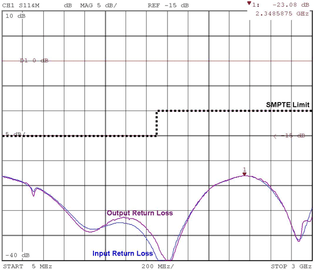
| RLIN | BNC_IO Return Loss | 5 MHz - 1.5 GHz(3)(9) | 15 | dB | ||
| 1.5 GHz - 3 GHz(3)(9) | 10 | dB | ||||
6.9 Output Mode (Cable Driver) AC Electrical Characteristics
Over Supply Voltage and Operating Temperature ranges, unless otherwise specified(2).| PARAMETER | TEST CONDITIONS | MIN | TYP | MAX | UNIT | |
|---|---|---|---|---|---|---|
| DRMAX | Maximum Input Data Rate | 2970 | Mbps | |||
| tjit | Additive Jitter | 2.97 Gbps(10) | 20 | psP-P | ||
| 1.485 Gbps(10) | 18 | psP-P | ||||
| 270 Mbps(10) | 15 | psP-P | ||||
| tr, tf | Output Rise Time, Fall Time | SD/HD = 0, 20% – 80% | 65 | 130 | ps | |
| SD/HD = 1, 20% – 80% | 400 | 800 | ps | |||
| Δtr, Δtf | Mismatch in Rise/Fall Time | SD/HD = 0 | 30 | ps | ||
| SD/HD = 1 | 50 | ps | ||||
| Duty Cycle Distortion | SD/HD = 0(3) | 30 | ps | |||
| SD/HD = 1(3) | 100 | ps | ||||
| tOS | Output Overshoot | SD/HD = 0(3) | 10% | |||
| SD/HD = 1(3) | 8% | |||||
| RLOUT | BNC_IO Output Return Loss | 5 MHz - 1.5 GHz(3)(9) | 15 | dB | ||
| 1.5 GHz - 3 GHz(3)(9) | 10 | dB | ||||
6.10 Input Mode (Equalizer) SPI Interface AC Electrical Characteristics
Over Supply Voltage and Operating Temperature ranges, unless otherwise specified (2).| PARAMETER | TEST CONDITIONS | MIN | TYP | MAX | UNIT | |
|---|---|---|---|---|---|---|
| fSCK | SCK Frequency | 20 | MHz | |||
| tPH | SCK Pulse Width High | Figure 2, Figure 3 | 40% | SCK period | ||
| tPL | SCK Pulse Width Low | 40% | SCK period | |||
| tSU | MOSI Setup Time | Figure 2, Figure 3 | 4 | ns | ||
| tH | MOSI Hold Time | 4 | ns | |||
| tSSSU | SS Setup Time | Figure 2, Figure 3 | 4 | ns | ||
| tSSH | SS Hold Time | 4 | ns | |||
| tSSOF | SS Off Time | 10 | ns | |||
| tODZ | MISO Driven-to-Tristate Time | Figure 3 | 15 | ns | ||
| tOZD | MISO Tristate-to-Driven Time | 15 | ns | |||
| tOD | MISO Output Delay Time | 15 | ns | |||
(1) Current flow into device pins is defined as positive. Current flow out of device pins is defined as negative. All voltages are stated referenced to VEE = 0 Volts.
(2) Typical values are stated for VCC = +3.3 V and TA = 25°C.
(3) Specification is ensured by characterization.
(4) The LMH0387 equalizer can be optimized for different launch amplitudes through the SPI.
(5) The differential output voltage and offset voltage are adjustable through the SPI.
(6) The equalizer automatically shifts equalization stages at cable lengths less than or equal to 120 m (Belden 1694A) to reduce power consumption. This power saving is also achieved by setting Extended 3G Reach Mode = 1 through the SPI. (Note: Forcing the Extended 3G Reach Mode in this way increases the cable reach for 3G data rates but also limits the achievable cable lengths at HD and SD data rates).
(7) Based on design and characterization data over the full range of recommended operating conditions of the device. Jitter is measured in accordance with ST RP 184, ST RP 192, and the applicable serial data transmission standard: ST 424, ST 292, or ST 259.
(8) LMH0387 equalizer launch amplitude fine tuning set to nominal through the SPI by writing 30h (“00110000 binary”) to SPI register 02h.
(9) Return loss is dependent on board design. The LMH0387 exceeds this specification on the SD387EVK evaluation board.
(10) Cable driver additive jitter is measured with the input AC coupled.
(11) Due to SMPTE naming convention, all SMPTE Engineering Documents will be numbered as a two-letter prefix and a number. Documents and references with the same root number and year are functionally identical; for example ST 424-2006 and SMPTE 424M-2006 refer to the same document.
 Figure 1. LVDS Output Voltage, Offset, and Timing Parameters
 Figure 2. SPI Write Operation
 Figure 3. SPI Read Operation
6.11 Typical Characteristics

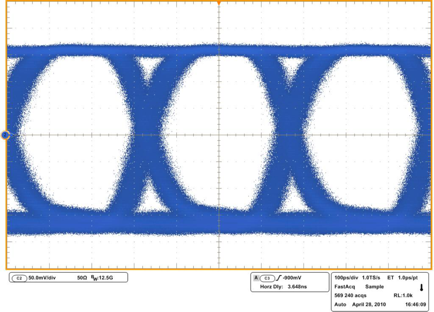
| 120m 0f B1694A at 2.97 Gbps, PRBS10 H: 100 ps / div, V: 50 mV / div (SDO Output Shown) |


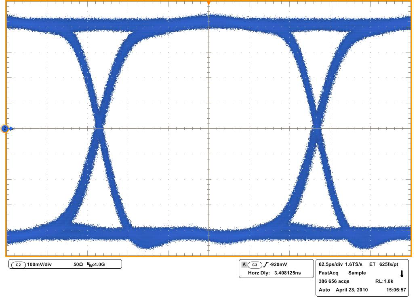
| H: 62.5 ps / div, V: 100 mV / div (BNC_IO Output Shown) | ||