SNLS312M August 2010 – July 2015 LMH0394
PRODUCTION DATA.
- 1 Features
- 2 Applications
- 3 Description
- 4 Revision History
- 5 Pin Configuration and Functions
- 6 Specifications
-
7 Detailed Description
- 7.1 Overview
- 7.2 Functional Block Diagram
- 7.3 Feature Description
- 7.4 Device Functional Modes
- 7.5
Programming
- 7.5.1
SPI Register Access
- 7.5.1.1 SPI Transaction Overview
- 7.5.1.2 SPI Write
- 7.5.1.3 SPI Read
- 7.5.1.4 SPI Daisy-Chain Operation
- 7.5.1.5 SPI Daisy-Chain Write
- 7.5.1.6 SPI Daisy-Chain Read
- 7.5.1.7 SPI Daisy-Chain Read and Write Example
- 7.5.1.8 SPI Daisy-Chain Length Detection
- 7.5.1.9 Output Driver Adjustments and De-emphasis Setting
- 7.5.1.10 Launch Amplitude Optimization
- 7.5.1.11 Cable Length Indicator (CLI)
- 7.5.1
SPI Register Access
- 7.6 Register Maps
- 8 Application and Implementation
- 9 Power Supply Recommendations
- 10Layout
- 11Device and Documentation Support
- 12Mechanical, Packaging, and Orderable Information
パッケージ・オプション
メカニカル・データ(パッケージ|ピン)
- RUM|16
サーマルパッド・メカニカル・データ
- RUM|16
発注情報
8 Application and Implementation
NOTE
Information in the following applications sections is not part of the TI component specification, and TI does not warrant its accuracy or completeness. TI’s customers are responsible for determining suitability of components for their purposes. Customers must validate and test their design implementation to confirm system functionality.
8.1 Application Information
The LMH0394 3-Gbps HD/SD SDI Low Power Extended Reach Adaptive Cable Equalizer is designed to equalize data transmitted over cable (or any media with similar dispersive loss characteristics). The equalizer operates over a wide range of data rates from 125 Mbps to 2.97 Gbps and supports ST 424, ST 292, ST 344, ST 259, and DVB-ASI standards. Additional features include separate carrier detect and output mute pins which may be tied together to mute the output when no signal is present. A programmable mute reference is provided to mute the output at a selectable level of signal degradation. The bypass pin allows the adaptive equalizer to be bypassed. The LMH0394 accepts single-ended input. The input must be AC coupled. The LMH0394 correctly handles equalizer pathological signals for standard definition and high definition serial digital video, as described in ST RP 178 and RP 198, respectively.
8.1.1 Interfacing to 3.3-V SPI
The LMH0394 may be controlled through optional SPI register access. The LMH0394 SPI pins support 2.5-V LVCMOS logic levels and are compliant with JEDEC JESD8-5 (see DC Electrical Characteristics). Care must be taken when interfacing the SPI pins to other voltage levels.
The 2.5-V LMH0394 SPI pins may be interfaced to a 3.3-V compliant SPI host by using a voltage divider or level translator. One implementation is a simple resistive voltage divider as shown in Figure 16.
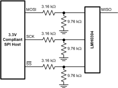 Figure 16. 3.3-V SPI Interfacing
8.1.2 Crosstalk Immunity
Single-ended SDI signals are susceptible to crosstalk and good design practices must be employed to minimize its effects. Most crosstalk originates through capacitive coupling from adjacent signals routed closely together through traces and connectors. To reduce capacitive coupling, SDI signals must be appropriately spaced apart or insulated from one another. This can be accomplished by physically isolating signal traces in the layout and by providing additional ground pins between signal traces in connectors as necessary. These techniques help to reduce crosstalk but do not eliminate it.
The LMH0394 was designed specifically with crosstalk in mind and incorporates advanced circuit design techniques that help to isolate and minimize the effects of cross-coupling in high-density system designs. The LMH0394’s enhanced design results in minimal degradation in cable reach in the presence of crosstalk and overall superior immunity against cross-coupling from neighboring channels.
8.2 Typical Application
Figure 17 shows the application circuit for the LMH0394 in SPI mode. (Note: The application circuit shows an external capacitor connected between the AEC+ and AEC- pins as commonly configured in legacy equalizers. This capacitor is optional and not necessary for the LMH0394; the AEC+ and AEC- pins may be left unconnected with no change in performance.)
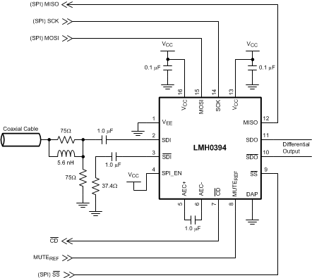 Figure 17. Application Circuit (SPI Mode)
8.2.1 Design Requirements
Table 2 lists the design parameters for the LMH0394.
Table 2. LMH0394 Design Parameters
| DESIGN PARAMETER | REQUIREMENT | |||
|---|---|---|---|---|
| Input AC coupling capacitors | Required. A common type of AC coupling capacitor is 1-µF ± 10% X7R ceramic capacitor (0402 or 0201 size). Capacitors may be implemented on the PCB or in the connector. | |||
| Distance from Device to BNC | Keep this distance as short as possible. | |||
| High-Speed SDI, and SDI trace impedance | Design single-ended trace impedance with 75 Ω ± 5% | |||
| High-Speed SDO, and SDO trace impedance | Design differential trace impedance with 100 Ω ± 5% | |||
| DC Power Supply Coupling Capacitors | To minimize power supply noise, use 0.01-µF capacitors as close to the device VDD pins as possible | |||
8.2.2 Detailed Design Procedure
To begin the design process, determine the following:
- Maximum power draw for PCB regulator selection: Use maximum current consumption in the data sheet.
- Closely compare schematic against typical connection diagram in the data sheet.
- Plan out the PCB layout and component placement to minimize parasitic.
- Consult the BNC vendor for optimum BNC landing pattern
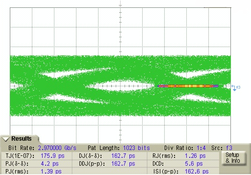
8.2.3 Application Curves
8.3 Do's and Dont's
Pay special attention to the PCB layout for the high-speed signals. SMPTE specifies the requirements for the Serial Digital Interface to transport digital video at SD, HD, and 3 Gbps data rates over coaxial cables. One of the requirements is meeting the required Return Loss. This requirement specifies how closely the port resembles 75-Ω impedance across a specified frequency band. The SMPTE specifications also defines the use of AC coupling capacitors for transporting uncompressed serial data streams with heavy low frequency content. This specification requires the use of a 1-µF AC coupling capacitor on the input of the LMH0394 to avoid low frequency bandwidth limitation.