SNWS020C November 2007 – October 2015 LMH2100
PRODUCTION DATA.
- 1 Features
- 2 Applications
- 3 Description
- 4 Revision History
- 5 Pin Configuration and Functions
- 6 Specifications
- 7 Detailed Description
- 8 Application and Implementation
- 9 Power Supply Recommendations
- 10Layout
- 11Device and Documentation Support
- 12Mechanical, Packaging, and Orderable Information
10 Layout
10.1 Layout Guidelines
As with any other RF device, careful attention must be paid to the board layout. If the board layout is not properly designed, unwanted signals can easily be detected or interference will be picked up. This section gives guidelines for proper board layout for the LMH2100.
Electrical signals (voltages and currents) need a finite time to travel through a trace or transmission line. RF voltage levels at the generator side and at the detector side can therefore be different. This is not only true for the RF strip line, but for all traces on the PCB. Signals at different locations or traces on the PCB will be in a different phase of the RF frequency cycle. Phase differences in, for example, the voltage across neighboring lines, may result in crosstalk between lines due to parasitic capacitive or inductive coupling. This crosstalk is further enhanced by the fact that all traces on the PCB are susceptible to resonance. The resonance frequency depends on the trace geometry. Traces are particularly sensitive to interference when the length of the trace corresponds to a quarter of the wavelength of the interfering signal or a multiple thereof.
10.1.1 Supply Lines
Because the PSRR of the LMH2100 is finite, variations of the supply can result in some variation at the output. This can be caused among others by RF injection from other parts of the circuitry or the on/off switching of the PA.
10.1.1.1 Positive Supply (VDD)
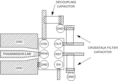
In order to minimize the injection of RF interference into the LMH2100 through the supply lines, the phase difference between the PCB traces connecting to VDD and GND should be minimized. A suitable way to achieve this is to short both connections for RF. This can be done by placing a small decoupling capacitor between the VDD and GND. It should be placed as close as possible to the VDD and GND pins of the LMH2100 as indicated in Figure 91. Be aware that the resonance frequency of the capacitor itself should be above the highest RF frequency used in the application, because the capacitor acts as an inductor above its resonance frequency.
Low frequency supply voltage variations due to PA switching might result in a ripple at the output voltage. The LMH2100 has a PSRR of 60 dB for low frequencies.
10.1.1.2 Ground (GND)
The LMH2100 needs a ground plane free of noise and other disturbing signals. It is important to separate the RF ground return path from the other grounds. This is due to the fact that the RF input handles large voltage swings. A power level of 0 dBm will cause a voltage swing larger than 0.6 VPP, over the internal 50-Ω input resistor. This will result in a significant RF return current toward the source. It is therefore recommended that the RF ground return path not be used for other circuits in the design. The RF path should be routed directly back to the source without loops.
10.1.2 RF Input Interface
The LMH2100 is designed to be used in RF applications, having a characteristic impedance of 50Ω. To achieve this impedance, the input of the LMH2100 needs to be connected via a 50Ω transmission line. Transmission lines can be easily created on PCBs using microstrip or (grounded) coplanar waveguide (GCPW) configurations. This section will discuss both configurations in a general way. For more details about designing microstrip or GCPW transmission lines, a microwave designer handbook is recommended.
10.1.3 Microstrip Configuration
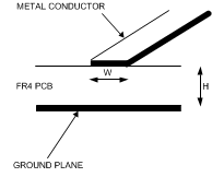
One way to create a transmission line is to use a microstrip configuration. A cross section of the configuration is shown in Figure 89, assuming a two-layer PCB.
 Figure 89. Microstrip Configuration
A conductor (trace) is placed on the topside of a PCB. The bottom side of the PCB has a fully copper ground plane. The characteristic impedance of the microstrip transmission line is a function of the width W, height H, and the dielectric constant εr.
Characteristics such as height and the dielectric constant of the board have significant impact on transmission line dimensions. A 50-Ω transmission line may result in impractically wide traces. A typical 1.6-mm thick FR4 board results in a trace width of 2.9 mm, for instance. This is impractical for the LMH2100 because the pad width of the 6-Bump DSBGA package is 0.24 mm. The transmission line has to be tapered from 2.9 mm to 0.24 mm. Significant reflections and resonances in the frequency transfer function of the board may occur due to this tapering.
10.1.4 GCPW Configuration
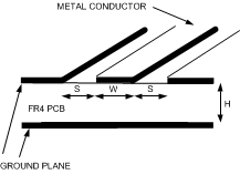
A transmission line in a (grounded) coplanar waveguide (GCPW) configuration will give more flexibility in terms of trace width. The GCPW configuration is constructed with a conductor surrounded by ground at a certain distance, S, on the top side. Figure 90 shows a cross section of this configuration. The bottom side of the PCB is a ground plane. The ground planes on both sides of the PCB should be firmly connected to each other by multiple vias. The characteristic impedance of the transmission line is mainly determined by the width W and the distance S. In order to minimize reflections, the width W of the center trace should match the size of the package pad. The required value for the characteristic impedance can subsequently be realized by selection of the proper gap width S.
 Figure 90. GCPW Configuration
10.1.5 Reference (REF)
The Reference pin can be used to compensate for temperature drift of the internal reference voltage as described in Interface to the ADC. The REF pin is directly connected to the inverting input of the transimpedance amplifier. Thus, RF signals and other spurious signals couple directly through to the output. Introduction of RF signals can be prevented by connecting a small capacitor between the REF pin and ground. The capacitor should be placed close to the REF pin as depicted in Figure 91.
10.1.6 Output (OUT)
The OUT pin is sensitive to crosstalk from the RF input, especially at high power levels. The ESD diode between OUT and VDD may rectify the crosstalk, but may add an unwanted inaccurate DC component to the output voltage.
The board layout should minimize crosstalk between the detectors input RFIN and the detectors output. Using an additional capacitor connected between the output and the positive supply voltage (VDD pin) or GND can prevent this. For optimal performance this capacitor should be placed as close as possible to the OUT pin of the LMH2100.
10.2 Layout Example
 Figure 91. Recommended LMH2100 Board Layout