JAJSEA6B December 2017 – February 2019 LMH5401-SP
PRODUCTION DATA.
- 1 特長
- 2 アプリケーション
- 3 概要
- 4 改訂履歴
- 5 概要(続き)
- 6 Pin Configuration and Functions
- 7 Specifications
-
8 Parameter Measurement Information
- 8.1 Output Reference Nodes and Gain Nomenclature
- 8.2 ATE Testing and DC Measurements
- 8.3 Frequency Response
- 8.4 S-Parameters
- 8.5 Frequency Response with Capacitive Load
- 8.6 Distortion
- 8.7 Noise Figure
- 8.8 Pulse Response, Slew Rate, and Overdrive Recovery
- 8.9 Power Down
- 8.10 VCM Frequency Response
- 8.11 Test Schematics
- 9 Detailed Description
-
10Application and Implementation
- 10.1 Application Information
- 10.2
Typical Application
- 10.2.1 Design Requirements
- 10.2.2 Detailed Design Procedure
- 10.2.3 Application Curves
- 10.3 Do's and Don'ts
- 11Power Supply Recommendations
- 12Layout
- 13デバイスおよびドキュメントのサポート
- 14メカニカル、パッケージ、および注文情報
10.2.2.4 Driving ADCs
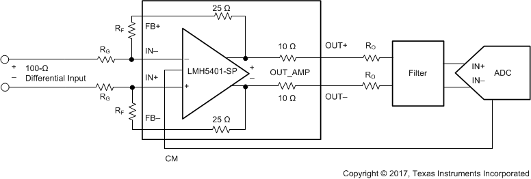
The LMH5401-SP is designed and optimized for the highest performance to drive differential input ADCs. Figure 67 shows a generic block diagram of the LMH5401-SP driving an ADC. The primary interface circuit between the amplifier and the ADC is usually a filter of some type for antialias purposes, and provides a means to bias the signal to the input common-mode voltage required by the ADC. Filters range from single-order real RC poles to higher-order LC filters, depending on the requirements of the application. Output resistors (RO) are shown on the amplifier outputs to isolate the amplifier from any capacitive loading presented by the filter.
 Figure 67. Differential ADC Driver Block Diagram
 The key points to consider for implementation are the SNR, SFDR, and ADC input considerations as described in this section.