JAJSEA6B December   2017  – February 2019 LMH5401-SP

PRODUCTION DATA.  

  1. 特長
  2. アプリケーション
  3. 概要
    1.     Device Images
      1.      LMH5401-SPの小信号周波数応答
      2.      LMH5401-SPによるADC12D1620QMLの駆動
  4. 改訂履歴
  5. 概要(続き)
  6. Pin Configuration and Functions
    1.     Pin Functions
  7. Specifications
    1. 7.1 Absolute Maximum Ratings
    2. 7.2 ESD Ratings
    3. 7.3 Recommended Operating Conditions
    4. 7.4 Thermal Information
    5. 7.5 Electrical Characteristics: VS = 5 V
    6. 7.6 Electrical Characteristics: VS = 3.3 V
    7. 7.7 Typical Characteristics: 5 V
    8. 7.8 Typical Characteristics: 3.3 V
  8. Parameter Measurement Information
    1. 8.1  Output Reference Nodes and Gain Nomenclature
    2. 8.2  ATE Testing and DC Measurements
    3. 8.3  Frequency Response
    4. 8.4  S-Parameters
    5. 8.5  Frequency Response with Capacitive Load
    6. 8.6  Distortion
    7. 8.7  Noise Figure
    8. 8.8  Pulse Response, Slew Rate, and Overdrive Recovery
    9. 8.9  Power Down
    10. 8.10 VCM Frequency Response
    11. 8.11 Test Schematics
  9. Detailed Description
    1. 9.1 Overview
    2. 9.2 Functional Block Diagram
    3. 9.3 Feature Description
      1. 9.3.1 Fully-Differential Amplifier
      2. 9.3.2 Operations for Single-Ended to Differential Signals
        1. 9.3.2.1 AC-Coupled Signal Path Considerations for Single-Ended Input to Differential Output Conversion
        2. 9.3.2.2 DC-Coupled Input Signal Path Considerations for SE-DE Conversions
        3. 9.3.2.3 Resistor Design Equations for Single-to-Differential Applications
        4. 9.3.2.4 Input Impedance Calculations
      3. 9.3.3 Differential-to-Differential Signals
        1. 9.3.3.1 AC-Coupled, Differential-Input to Differential-Output Design Issues
        2. 9.3.3.2 DC-Coupled, Differential-Input to Differential-Output Design Issues
      4. 9.3.4 Output Common-Mode Voltage
    4. 9.4 Device Functional Modes
      1. 9.4.1 Operation With a Split Supply
      2. 9.4.2 Operation With a Single Supply
  10. 10Application and Implementation
    1. 10.1 Application Information
      1. 10.1.1 Stability, Noise Gain, and Signal Gain
      2. 10.1.2 Input and Output Headroom Considerations
      3. 10.1.3 Noise Analysis
      4. 10.1.4 Noise Figure
      5. 10.1.5 Thermal Considerations
    2. 10.2 Typical Application
      1. 10.2.1 Design Requirements
      2. 10.2.2 Detailed Design Procedure
        1. 10.2.2.1 Driving Matched Loads
        2. 10.2.2.2 Driving Unmatched Loads For Lower Loss
        3. 10.2.2.3 Driving Capacitive Loads
        4. 10.2.2.4 Driving ADCs
          1. 10.2.2.4.1 SNR Considerations
          2. 10.2.2.4.2 SFDR Considerations
          3. 10.2.2.4.3 ADC Input Common-Mode Voltage Considerations—AC-Coupled Input
          4. 10.2.2.4.4 ADC Input Common-Mode Voltage Considerations—DC-Coupled Input
        5. 10.2.2.5 GSPS ADC Driver
        6. 10.2.2.6 Common-Mode Voltage Correction
        7. 10.2.2.7 Active Balun
      3. 10.2.3 Application Curves
    3. 10.3 Do's and Don'ts
      1. 10.3.1 Do:
      2. 10.3.2 Don't:
  11. 11Power Supply Recommendations
    1. 11.1 Supply Voltage
    2. 11.2 Single Supply
    3. 11.3 Split Supply
    4. 11.4 Supply Decoupling
  12. 12Layout
    1. 12.1 Layout Guidelines
    2. 12.2 Layout Example
  13. 13デバイスおよびドキュメントのサポート
    1. 13.1 デバイス・サポート
      1. 13.1.1 デバイスの項目表記
    2. 13.2 ドキュメントのサポート
      1. 13.2.1 関連資料
    3. 13.3 ドキュメントの更新通知を受け取る方法
    4. 13.4 コミュニティ・リソース
    5. 13.5 商標
    6. 13.6 静電気放電に関する注意事項
    7. 13.7 Glossary
  14. 14メカニカル、パッケージ、および注文情報

パッケージ・オプション

メカニカル・データ(パッケージ|ピン)
サーマルパッド・メカニカル・データ
発注情報

ADC Input Common-Mode Voltage Considerations—AC-Coupled Input

The input common-mode voltage range of the ADC must be respected for proper operation. In an ac-coupled application between the amplifier and the ADC, the input common-mode voltage bias of the ADC is accomplished in different ways depending on the ADC. Some ADCs use internal bias networks such that the analog inputs are automatically biased to the required input common-mode voltage if the inputs are ac-coupled with capacitors (or if the filter between the amplifier and ADC is a band-pass filter). Other ADCs supply their required input common-mode voltage from a reference voltage output pin (often called CM or VCM). With these ADCs, the ac-coupled input signal can be re-biased to the input common-mode voltage by connecting resistors from each input to the CM output of the ADC, as Figure 68 shows. However, the signal is attenuated because of the voltage divider created by RCM and RO.
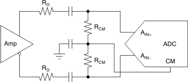
LMH5401-SP ai_bias_bos520.gifFigure 68. Biasing AC-Coupled ADC Inputs Using the ADC CM Output

The signal can be re-biased when ac coupling; thus, the output common-mode voltage of the amplifier is a don’t care for the ADC.