SNOSB47E May 2011 – August 2016 LMH6521
PRODUCTION DATA.
- 1 Features
- 2 Applications
- 3 Description
- 4 Revision History
- 5 Pin Configuration and Functions
- 6 Specifications
- 7 Detailed Description
- 8 Application and Implementation
- 9 Power Supply Recommendations
- 10Layout
- 11Device and Documentation Support
- 12Mechanical, Packaging, and Orderable Information
パッケージ・オプション
メカニカル・データ(パッケージ|ピン)
- RTV|32
サーマルパッド・メカニカル・データ
- RTV|32
発注情報
8 Application and Implementation
NOTE
Information in the following applications sections is not part of the TI component specification, and TI does not warrant its accuracy or completeness. TI’s customers are responsible for determining suitability of components for their purposes. Customers should validate and test their design implementation to confirm system functionality.
8.1 Application Information
Common applications for the LMH6521 would be an IF amplifier, RF amplifier, and ADC driver.
Many applications require impedance matching and filtering. The large voltage swing of the LMH6521 makes it ideal for use with a filter.
The LMH6521 is ideal for applications requiring variable gain and very high linearity for frequencies ranging from 1 MHz to 500 MHz. The LMH6521 can support output voltage swing up to 10 VPP.
8.2 Typical Application
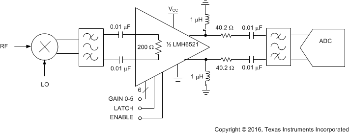
The most typical application for the LMH5621 is shown in Figure 38. In this application the LMH6521 is driving an ADC through a band pass filter.
 Figure 38. ADC Driver Application
8.2.1 Design Requirements
An ADC driver is required to deliver a full-scale signal to the ADC input pins with harmonic and intermodulation distortion products that meet the system requirements.
In this example we want to meet the following requirements:
- Amplifier output voltage: 4 VPP
- SFDR > 80 dB at 300 MHz
- Noise voltage < 0 nV/rt Hz
8.2.2 Detailed Design Procedure
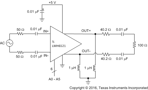
A voltage between 4.75 V and 5.25 V must be applied to the supply pin labeled 5 V. Each supply pin must be decoupled with a additional capacitance along with some low inductance, surface-mount ceramic capacitor of 0.01 µF as close to the device as possible where space allows.
The outputs of the LMH6521 are low impedance devices that requires connection to ground with 1-µH RF chokes and require AC-coupling capacitors of 0.01 µF. The input pins are self biased to 2.5 V and must be ac-coupled with 0.01-µF capacitors as well. The output RF inductors and AC-coupling capacitors are the main limitations for operating at low frequencies.
Each channel of the LMH6521 consists of a digital step attenuator followed by a low-distortion, 26-dB fixed gain amplifier and a low impedance output stage. The gain is digitally controlled over a 31.5-dB range from 26 dB to −5.5 dB. The LMH6521 has a 200-Ω differential input impedance and a low 20-Ω differential output impedance.
To enable each channel of the LMH6521, the ENA and ENB pins can be left to float, which internally is connected high with a weak pullup resistor. Externally connecting ENA and ENB to ground disables the channels of the LMH6521 and reduce the current consumption to 17.5 mA per channel.
 Figure 39. Basic Operating Connection
The LMH6521 meets the SFDR and output voltage swing requirements with no additional design details. However, the noise requires an additional filter as shown in Figure 38. The filter termination reduces the LMH6521 output noise voltage from 33 nV/rt Hz to 16.5 nV/rt Hz. A simple third order filter reduces out of band noise that would alias into the signal path. For filter details, see Interface to ADC.
 Figure 40. Filter Schematic
For further design assistance, see SP16160CH1RB Reference Design Board User’s Guide (SNAU079).
8.2.3 Application Curve
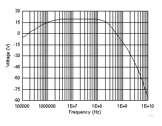
 Figure 41. Filter Frequency Response