SNCS104D April 2005 – December 2014 LMH6570
PRODUCTION DATA.
6 Specifications
6.1 Absolute Maximum Ratings(1)(1)
| MIN | MAX | UNIT | ||
|---|---|---|---|---|
| Supply Voltage (V+ − V−) | 13.2 | V | ||
| IOUT(3) | 130 | mA | ||
| Signal & Logic Input Pin Voltage | ±(VS + 0.6) | V | ||
| Signal & Logic Input Pin Current | ±20 | mA | ||
| Maximum Junction Temperature | +150 | °C | ||
| Storage Temperature | −65 | +150 | °C | |
| Soldering Information | Infrared or Convection (20 sec) | 235 | °C | |
| Wave Soldering (10 sec) | 260 | °C | ||
(1) If Military/Aerospace specified devices are required, please contact the Texas Instruments Sales Office/ Distributors for availability and specifications.
6.2 ESD Ratings
| VALUE | UNIT | |||
|---|---|---|---|---|
| V(ESD) | Electrostatic discharge | Human-body model (HBM), per ANSI/ESDA/JEDEC JS-001(1) | ±2000 | V |
| Machine model (MM)(2) | ±200 | |||
(1) JEDEC document JEP155 states that 500-V HBM allows safe manufacturing with a standard ESD control process. Manufacturing with less than 500-V HBM is possible with the necessary precautions. Pins listed as ±2000 V may actually have higher performance. Human body model, 1.5kΩ in series with 100 pF.
(2) Machine model, 0 Ω In series with 200 pF
6.3 Recommended Operating Conditions
over operating free-air temperature range (unless otherwise noted)| MIN | NOM | MAX | UNIT | ||
|---|---|---|---|---|---|
| Operating Temperature | −40 | 85 | °C | ||
| Supply Voltage | 6 | 12 | V | ||
6.4 Thermal Information
| THERMAL METRIC(1) | D | UNIT | |
|---|---|---|---|
| 8 PINS | |||
| RθJA | Junction-to-ambient thermal resistance | 150 | °C/W |
| RθJC(top) | Junction-to-case (top) thermal resistance | 50 | |
(1) For more information about traditional and new thermal metrics, see the IC Package Thermal Metrics application report, SPRA953.
6.5 Electrical Characteristics ±5V
VS = ±5 V, RL = 100 Ω, RF = 576 Ω, AV = 2 V/V, TJ = 25 °C, unless otherwise specified.| PARAMETER | TEST CONDITIONS(2) | MIN(4) | TYP(8) | MAX(4) | UNIT | ||
|---|---|---|---|---|---|---|---|
| FREQUENCY DOMAIN PERFORMANCE | |||||||
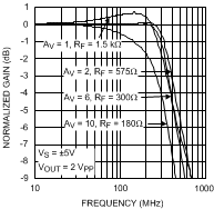
| SSBW | −3 dB Bandwidth | VOUT = 0.5 VPP | 500 | MHz | |||
| LSBW | –3 dB Bandwidth | VOUT = 2 VPP(5) | 400 | MHz | |||
| .1 dBBW | 0.1 dB Bandwidth | VOUT = 0.25 VPP | 150 | MHz | |||
| DG | Differential gain | RL = 150 Ω, f = 4.43 MHz | 0.02% | ||||
| DP | Differential phase | RL = 150 Ω, f = 4.43 MHz | 0.05 | deg | |||
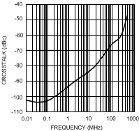
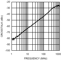
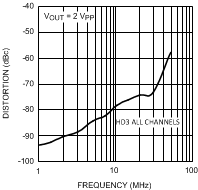
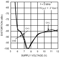
| XTLK | Channel to channel crosstalk | All Hostile, f = 5 MHz | −70 | dBc | |||
| TIME DOMAIN RESPONSE | |||||||
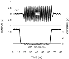
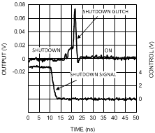
| TRS | Channel to channel switching time | Logic transition to 90% output | 8 | ns | |||
| Enable and disable times | Logic transition to 90% or 10% output. | 10 | ns | ||||
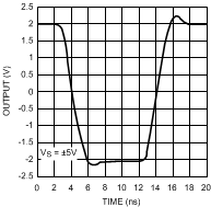
| TRL | Rise and fall time | 4 V Step | 2.4 | ns | |||
| TSS | Settling time to 0.05% | 2 V Step | 17 | ns | |||
| OS | Overshoot | 2 V Step | 5% | ||||
| SR | Slew rate | 4 V Step(5)(7) | 2200 | V/μs | |||
| DISTORTION | |||||||
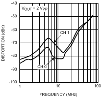
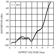
| HD2 | 2nd Harmonic distortion | 2 VPP , 5 MHz | −68 | dBc | |||
| HD3 | 3rd Harmonic distortion | 2 VPP , 5 MHz | −84 | dBc | |||
| IMD | 3rd Order intermodulation products | 10 MHz, Two tones 2 Vpp at output | −80 | dBc | |||
| EQUIVALENT INPUT NOISE | |||||||
| VN | Voltage | >1 MHz, Input Referred | 5 | nV√HZ | |||
| ICN | Current | >1 MHz, Input Referred | 5 | pA/√Hz | |||
| STATIC, DC PERFORMANCE | |||||||
| CHGM | Channel to channel gain difference | DC, Difference in gain between channels | ±0.005% | ±0.034% | |||
| -40°C ≤ TJ ≤ 85°C | ±0.036% | ||||||
| VIO | Input offset voltage | VIN = 0 V | 1 | ±15 | mV | ||
| -40°C ≤ TJ ≤ 85°C | ±21 | ||||||
| DVIO | Offset voltage drift(9) | 30 | µV/°C | ||||
| IBN | Input bias current(6) | VIN = 0 V | −3 | ±8 | µA | ||
| -40°C ≤ TJ ≤ 85°C | ±10 | ||||||
| DIBN | Bias current drift(9) | 11 | nA/°C | ||||
| IBI | Inverting input bias current(6) | Pin 8, Feedback point, VIN = 0 V |
−3 | ±18 | uA | ||
| -40°C ≤ TJ ≤ 85°C | ±22 | ||||||
| PSRR | Power supply rejection ratio |
DC, Input referred | 48 | 50 | dB | ||
| -40°C ≤ TJ ≤ 85°C | 46 | ||||||
| ICC | Supply current | No Load, Shutdown Pin (SD) > 0.8 V | 13.8 | 15 | mA | ||
| -40°C ≤ TJ ≤ 85°C | 16 | ||||||
| Supply current shutdown | Shutdown Pin (SD) > 2 V | 1.1 | 1.3 | mA | |||
| -40°C ≤ TJ ≤ 85°C | 1.4 | ||||||
| VIH | Logic high threshold | Select Pin & Shutdown pin (SEL, SD) | 2.0 | V | |||
| VIL | Logic low threshold | Select Pin & Shutdown pin (SEL, SD) | 0.8 | V | |||
| IiL | Logic pin input current low(6) | Logic Input = 0 V Select Pin & Shutdown Pin (SEL, SD) | −8 | −1 | µA | ||
| -40°C ≤ TJ ≤ 85°C | -10 | ||||||
| IiH | Logic pin input current high(6) | Logic Input = 5.0 V, Select Pin & Shutdown Pin (SEL, SD) | 57 | 68 | µA | ||
| -40°C ≤ TJ ≤ 85°C | 75 | ||||||
| MISCELLANEOUS PERFORMANCE | |||||||
| RIN+ | Input resistance | 5 | kΩ | ||||
| CIN | Input capacitance | 0.8 | pF | ||||
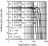
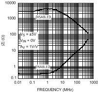
| ROUT | Output resistance | Output Active, (SD < 0.8 V) | 0.04 | Ω | |||
| ROUT | Output resistance | Output Disabled, (SD > 2 V) | 3000 | Ω | |||
| COUT | Output capacitance | Output Disabled, (SD > 2 V) | 3.1 | pF | |||
| VO | Output voltage range | No Load | ±3.51 | ±3.7 | V | ||
| -40°C ≤ TJ ≤ 85°C | ±3.50 | ||||||
| VOL | RL = 100 Ω | ±3.16 | ±3.5 | V | |||
| -40°C ≤ TJ ≤ 85°C | ±3.15 | ||||||
| CMIR | Input voltage range | ±2.5 | ±2.6 | V | |||
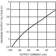
| IO | Linear output current(6) | VIN = 0 V | +60 | ±80 | mA | ||
| -70 | |||||||
| -40°C ≤ TJ ≤ 85°C | ±55 | ||||||
| ISC | Short circuit current(3) | VIN = ±2 V, Output shorted to ground | ±230 | mA | |||
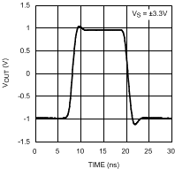
6.6 Electrical Characteristics ±3.3V
VS = ±3.3 V, RL = 100 Ω, RF = 576 Ω, AV = 2 V/V, unless otherwise specified.| PARAMETER | TEST CONDITIONS(2) | MIN(4) | TYP(8) | MAX(4) | UNIT | |
|---|---|---|---|---|---|---|
| FREQUENCY DOMAIN PERFORMANCE | ||||||
| SSBW | −3 dB Bandwidth | VOUT = 0.5 VPP | 475 | MHz | ||
| LSBW | −3 dB Bandwidth | VOUT = 2.0 VPP | 375 | MHz | ||
| 0.1 dBBW | 0.1 dB Bandwidth | VOUT = 0.5 VPP | 100 | MHz | ||
| GFP | Peaking | DC to 200 MHz | 0.4 | dB | ||
| XTLK | Channel to channel crosstalk | All Hostile, f = 5 MHz | −70 | dBc | ||
| TIME DOMAIN RESPONSE | ||||||
| TRL | Rise and Fall time | 2 V Step | 2 | ns | ||
| TSS | Settling time to 0.05% | 2 V Step | 20 | ns | ||
| OS | Overshoot | 2 V Step | 5% | |||
| SR | Slew rate | 2 V Step | 1400 | V/μs | ||
| DISTORTION | ||||||
| HD2 | 2nd Harmonic distortion | 2 VPP, 10 MHz | −67 | dBc | ||
| HD3 | 3rd Harmonic distortion | 2 VPP, 10 MHz | −87 | dBc | ||
| STATIC, DC PERFORMANCE | ||||||
| VIO | Input offset voltage | VIN = 0 V | 1 | mV | ||
| IBN | Input bias current(6) | VIN = 0 V | -3 | μA | ||
| PSRR | Power supply rejection ratio | DC, Input Referred | 49 | dB | ||
| ICC | Supply current | No Load | 12.5 | mA | ||
| VIH | Logic high threshold | Select Pin & Shutdown pin (SEL, SD), VIH ≊ V+ * 0.4 |
1.3 | V | ||
| VIL | Logic low threshold | Select Pin & Shutdown pin (SEL, SD), VIL ≊ V+ * 0.12 |
0.4 | V | ||
| MISCELLANEOUS PERFORMANCE | ||||||
| RIN+ | Input resistance | 5 | kΩ | |||
| CIN | Input capacitance | 0.8 | pF | |||
| ROUT | Output resistance | 0.06 | Ω | |||
| VO | Output voltage range | No Load | ±2 | V | ||
| VOL | RL = 100 Ω | ±1.8 | V | |||
| CMIR | Input voltage range | ±1.2 | V | |||
| IO | Linear output current(3) | VIN = 0 V | ±60 | mA | ||
| ISC | Short circuit current(3) | VIN = ±1 V, Output shorted to ground | ±150 | mA | ||
(1) Absolute Maximum Ratings indicate limits beyond which damage to the device may occur. Operating Ratings indicate conditions for which the device is intended to be functional, but specific performance is not ensured. For specifications, see the Electrical Characteristics tables.
(2) Electrical Table values apply only for factory testing conditions at the temperature indicated. Factory testing conditions result in very limited self-heating of the device such that TJ = TA. No specification of parametric performance is indicated in the electrical tables under conditions of internal self heating where TJ > TA. See Thermal Information for information on temperature de-rating of this device. Min/Max ratings are based on product testing, characterization and simulation. Individual parameters are tested as noted.
(3) The maximum output current (IOUT) is determined by the device power dissipation limitations (The junction temperature cannot be allowed to exceed 150°C). See Power Dissipation for more details. A short circuit condition should be limited to 5 seconds or less.
(4) Limits are 100% production tested at 25°C. Limits over the operating temperature range are ensured through correlation using Statistical Quality Control (SQC) methods.
(5) Parameter ensured by design.
(6) Positive Value is current into device.
(7) Slew Rate is the average of the rising and falling edges.
(8) Typical numbers are the most likely parametric norm.
(9) Drift determined by dividing the change in parameter at temperature extremes by the total temperature change.
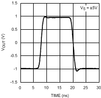
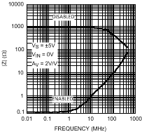
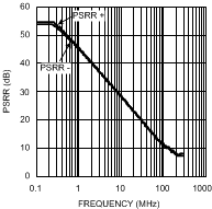
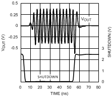
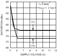
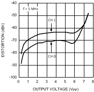
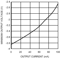
6.7 Typical Performance Characteristics
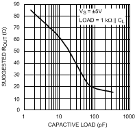
Vs = ±5 V, RL = 100 Ω, AV = 2, RF = RG = 576 Ω, unless otherwise specified.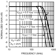
| Positive value is current into device | ||
| Positive value is current into device | ||