JAJSQ22J september 2011 – may 2023 LMK00301
PRODUCTION DATA
- 1
- 1 特長
- 2 アプリケーション
- 3 概要
- 4 Revision History
- 5 Device Comparison
- 6 Pin Configuration and Functions
- 7 Specifications
- 8 Parameter Measurement Information
- 9 Detailed Description
- 10Application and Implementation
- 11Power Supply Recommendations
- 12Layout
- 13Device and Documentation Support
- 14Mechanical, Packaging, and Orderable Information
パッケージ・オプション
メカニカル・データ(パッケージ|ピン)
- RHS|48
サーマルパッド・メカニカル・データ
- RHS|48
発注情報
10.2.2.1.1 Termination for DC Coupled Differential Operation
For DC coupled operation of an LVDS driver, terminate with 100 Ω as close as possible to the LVDS receiver as shown in Figure 10-6.
 Figure 10-6 Differential LVDS Operation, DC Coupling, No Biasing by the Receiver
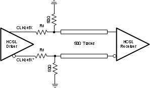
For DC coupled operation of an HCSL driver, terminate with 50 Ω to ground near the driver output as shown in Figure 10-7. Series resistors, Rs, may be used to limit overshoot due to the fast transient current. Because HCSL drivers require a DC path to ground, AC coupling is not allowed between the output drivers and the 50 Ω termination resistors.
 Figure 10-7 HCSL Operation, DC Coupling
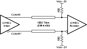
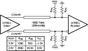
For DC coupled operation of an LVPECL driver, terminate with 50 Ω to Vcco - 2 V as shown in Figure 10-8. Alternatively terminate with a Thevenin equivalent circuit as shown in Figure 10-9 for Vcco (output driver supply voltage) = 3.3 V and 2.5 V. In the Thevenin equivalent circuit, the resistor dividers set the output termination voltage (VTT) to Vcco - 2 V.
 Figure 10-8 Differential LVPECL Operation, DC Coupling
 Figure 10-9 Differential LVPECL Operation, DC Coupling, Thevenin Equivalent