SNAS578D February 2012 – March 2016 LMK00306
PRODUCTION DATA.
- 1 Features
- 2 Applications
- 3 Description
- 4 Revision History
- 5 Pin Configuration and Functions
- 6 Specifications
- 7 Parameter Measurement Information
- 8 Detailed Description
- 9 Application and Implementation
- 10Power Supply Recommendations
- 11Device and Documentation Support
- 12Mechanical, Packaging, and Orderable Information
パッケージ・オプション
デバイスごとのパッケージ図は、PDF版データシートをご参照ください。
メカニカル・データ(パッケージ|ピン)
- NJK|36
サーマルパッド・メカニカル・データ
発注情報
8 Detailed Description
8.1 Overview
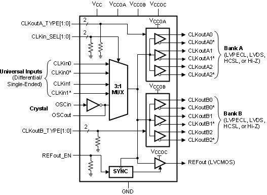
The LMK00306 is a 6-output differential clock fanout buffer with low additive jitter that can operate up to 3.1 GHz. It features a 3:1 input multiplexer with an optional crystal oscillator input, two banks of 3 differential outputs with multi-mode buffers (LVPECL, LVDS, HCSL, or Hi-Z), one LVCMOS output, and 3 independent output buffer supplies. The input selection and output buffer modes are controlled via pin strapping. The device is offered in a 36-pin WQFN package and leverages much of the high-speed, low-noise circuit design employed in the LMK04800 family of clock conditioners.
8.2 Functional Block Diagram

8.3 Feature Description
8.3.1 VCC and VCCO Power Supplies
The LMK00306 has separate 3.3 V core supply (VCC) and 3 independent 3.3 V/2.5 V output power supplies (VCCOA, VCCOB, VCCOC). Output supply operation at 2.5 V enables lower power consumption and output-level compatibility with 2.5 V receiver devices. The output levels for LVPECL (VOH, VOL) and LVCMOS (VOH) are referenced to the respective Vcco supply, while the output levels for LVDS and HCSL are relatively constant over the specified Vcco range. Refer to Power Supply Recommendations for additional supply related considerations, such as power dissipation, power supply bypassing, and power supply ripple rejection (PSRR).
NOTE
Care should be taken to ensure the Vcco voltages do not exceed the Vcc voltage to prevent turning-on the internal ESD protection circuitry.
8.3.2 Clock Inputs
The input clock can be selected from CLKin0/CLKin0*, CLKin1/CLKin1*, or OSCin. Clock input selection is controlled using the CLKin_SEL[1:0] inputs as shown in Table 2 . Refer to Driving the Clock Inputs for clock input requirements. When CLKin0 or CLKin1 is selected, the crystal circuit is powered down. When OSCin is selected, the crystal oscillator circuit will start-up and its clock will be distributed to all outputs. Refer to Crystal Interface for more information. Alternatively, OSCin may be be driven by a single-ended clock (up to 250 MHz) instead of a crystal.
Table 2. Input Selection
| CLKin_SEL1 | CLKin_SEL0 | SELECTED INPUT |
|---|---|---|
| 0 | 0 | CLKin0, CLKin0* |
| 0 | 1 | CLKin1, CLKin1* |
| 1 | X | OSCin |
Table 3 shows the output logic state vs. input state when either CLKin0/CLKin0* or CLKin1/CLKin1* is selected. When OSCin is selected, the output state will be an inverted copy of the OSCin input state.
Table 3. CLKin Input vs. Output States
| STATE of SELECTED CLKin |
STATE of ENABLED OUTPUTS |
|---|---|
| CLKinX and CLKinX* inputs floating |
Logic low |
| CLKinX and CLKinX* inputs shorted together |
Logic low |
| CLKin logic low | Logic low |
| CLKin logic high | Logic high |
8.3.3 Clock Outputs
The differential output buffer type for Bank A and Bank B outputs can be separately configured using the CLKoutA_TYPE[1:0] and CLKoutB_TYPE[1:0] inputs, respectively, as shown in Table 4. For applications where all differential outputs are not needed, any unused output pin should be left floating with a minimum copper length (see note below) to minimize capacitance and potential coupling and reduce power consumption. If an entire output bank will not be used, it is recommended to disable/Hi-Z the bank to reduce power. Refer to Termination and Use of Clock Drivers for more information on output interface and termination techniques.
NOTE
For best soldering practices, the minimum trace length for any unused output pin should extend to include the pin solder mask. This way during reflow, the solder has the same copper area as connected pins. This allows for good, uniform fillet solder joints helping to keep the IC level during reflow.
Table 4. Differential Output Buffer Type Selection
| CLKoutX_ TYPE1 |
CLKoutX_ TYPE0 |
CLKoutX BUFFER TYPE (BANK A or B) |
|---|---|---|
| 0 | 0 | LVPECL |
| 0 | 1 | LVDS |
| 1 | 0 | HCSL |
| 1 | 1 | Disabled (Hi-Z) |
8.3.3.1 Reference Output
The reference output (REFout) provides a LVCMOS copy of the selected input clock. The LVCMOS output high level is referenced to the Vcco voltage. REFout can be enabled or disabled using the enable input pin, REFout_EN, as shown in Table 5.
Table 5. Reference Output Enable
| REFout_EN | REFout State |
|---|---|
| 0 | Disabled (Hi-Z) |
| 1 | Enabled |
The REFout_EN input is internally synchronized with the selected input clock by the SYNC block. This synchronizing function prevents glitches and runt pulses from occurring on the REFout clock when enabled or disabled. REFout will be enabled within 3 cycles (tEN) of the input clock after REFout_EN is toggled high. REFout will be disabled within 3 cycles (tDIS) of the input clock after REFout_EN is toggled low.
When REFout is disabled, the use of a resistive loading can be used to set the output to a predetermined level. For example, if REFout is configured with a 1 kΩ load to ground, then the output will be pulled to low when disabled.