JAJSFC0E December   2013  – January 2022 LMK00334

PRODUCTION DATA  

  1. 特長
  2. アプリケーション
  3. 概要
  4. Revision History
  5. Pin Configuration and Functions
  6. Specifications
    1. 6.1 Absolute Maximum Ratings
    2. 6.2 ESD Ratings
    3. 6.3 Recommended Operating Conditions
    4. 6.4 Thermal Information
    5. 6.5 Electrical Characteristics
    6. 6.6 Timing Requirements, Propagation Delay, and Output Skew
    7. 6.7 Typical Characteristics
  7. Parameter Measurement Information
    1. 7.1 Differential Voltage Measurement Terminology
  8. Detailed Description
    1. 8.1 Overview
    2. 8.2 Functional Block Diagram
    3. 8.3 Feature Description
      1. 8.3.1 Crystal Power Dissipation vs. RLIM
      2. 8.3.2 Clock Inputs
      3. 8.3.3 Clock Outputs
        1. 8.3.3.1 Reference Output
    4. 8.4 Device Functional Modes
      1. 8.4.1 VCC and VCCO Power Supplies
  9. Application and Implementation
    1. 9.1 Application Information
    2. 9.2 Typical Application
      1. 9.2.1 Design Requirements
        1. 9.2.1.1 Driving the Clock Inputs
        2. 9.2.1.2 Crystal Interface
      2. 9.2.2 Detailed Design Procedure
        1. 9.2.2.1 Termination and Use of Clock Drivers
        2. 9.2.2.2 Termination for DC-Coupled Differential Operation
        3. 9.2.2.3 Termination for AC-Coupled Differential Operation
      3. 9.2.3 Application Curve
  10. 10Power Supply Recommendations
    1. 10.1 Current Consumption and Power Dissipation Calculations
      1. 10.1.1 Power Dissipation Example: Worst-Case Dissipation
    2. 10.2 Power Supply Bypassing
      1. 10.2.1 Power Supply Ripple Rejection
  11. 11Layout
    1. 11.1 Layout Guidelines
    2. 11.2 Layout Example
    3. 11.3 Thermal Management
  12. 12Device and Documentation Support
    1. 12.1 Documentation Support
      1. 12.1.1 Related Documentation
    2. 12.2 Receiving Notification of Documentation Updates
    3. 12.3 サポート・リソース
    4. 12.4 Trademarks
    5. 12.5 Electrostatic Discharge Caution
    6. 12.6 Glossary
  13. 13Mechanical, Packaging, and Orderable Information

パッケージ・オプション

メカニカル・データ(パッケージ|ピン)
サーマルパッド・メカニカル・データ
発注情報

Typical Characteristics

Unless otherwise specified: VCC = 3.3 V, VCCO = 3.3 V, TA = 25°C, CLKin driven differentially, input slew rate ≥ 3 V/ns.
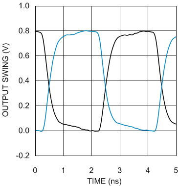
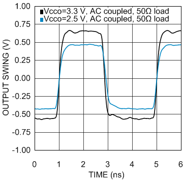
GUID-B73333E8-B543-4292-A53D-E6C3C9609544-low.gifFigure 6-1 HCSL Output Swing at 250 MHz
GUID-D91D4248-117D-4AE6-A8CE-A6F97B697B69-low.gif
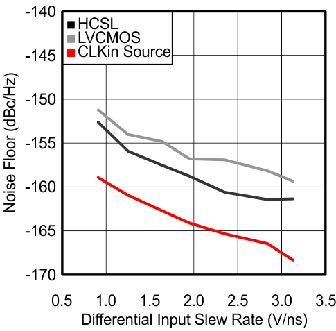
Fclk = 100 MHz Foffset = 20 MHz
Figure 6-3 Noise Floor vs. CLKin Slew Rate at 100 MHz
GUID-7F71D43A-46BE-4354-9644-71C6B9969444-low.gif
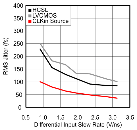
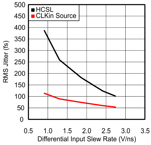
Fclk = 100 MHz Int. BW = 1 to 20 MHz
Figure 6-5 RMS Jitter vs. CLKin Slew Rate at 100 MHz
GUID-A5EDDC74-34A1-4A62-B10C-AC93FACDA0AA-low.gif
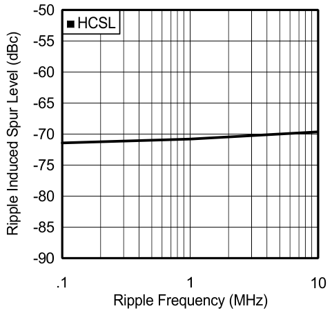
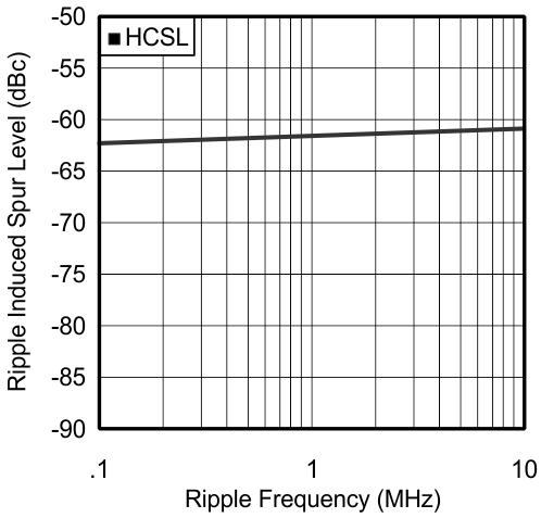
Fclk = 156.25 MHz Vccco Ripple = 100 mVpp
Figure 6-7 PSRR vs. Ripple Frequency at 156.25 MHz
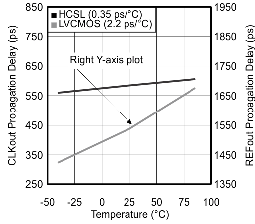
GUID-EDA354D4-64DC-4DFE-9800-8455480E8714-low.gifFigure 6-9 Propagation Delay vs. Temperature
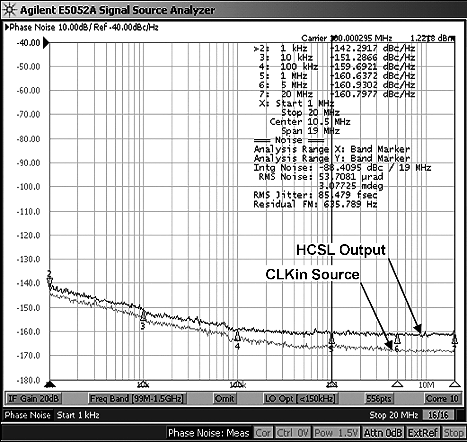
GUID-DE33A75A-AC41-47EE-9C44-50576D691209-low.pngFigure 6-11 HCSL Phase Noise at 100 MHz
GUID-B13EADB1-DB07-47D1-A2BE-807159A3F869-low.gifFigure 6-2 LVCMOS Output Swing at 250 MHz
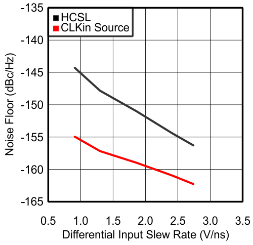
GUID-D106D3BB-59BC-400C-B510-4A4D2F7EE423-low.gif
Fclk = 156.25 MHz Foffset = 20 MHz
Figure 6-4 Noise Floor vs. CLKin Slew Rate at 156.25 MHz
GUID-E787D580-48A0-4CCD-BE1F-EFFE3CE13412-low.gif
Fclk = 156.25 MHz Int. BW = 1 to 20 MHz
Figure 6-6 RMS Jitter vs. CLKin Slew Rate at 156.25 MHz
GUID-50E84E33-3EDC-4AF9-80E4-26232B6B9CBE-low.gif
Fclk = 312.5 MHz Vccco Ripple = 100 mVpp
Figure 6-8 PSRR vs. Ripple Frequency at 312.5 MHz
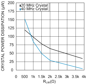
GUID-AF646A5B-A943-49F4-BEC9-A113BD57E701-low.gifFigure 6-10 Crystal Power Dissipation vs. RLIM