JAJSFC0E December   2013  – January 2022 LMK00334

PRODUCTION DATA  

  1. 特長
  2. アプリケーション
  3. 概要
  4. Revision History
  5. Pin Configuration and Functions
  6. Specifications
    1. 6.1 Absolute Maximum Ratings
    2. 6.2 ESD Ratings
    3. 6.3 Recommended Operating Conditions
    4. 6.4 Thermal Information
    5. 6.5 Electrical Characteristics
    6. 6.6 Timing Requirements, Propagation Delay, and Output Skew
    7. 6.7 Typical Characteristics
  7. Parameter Measurement Information
    1. 7.1 Differential Voltage Measurement Terminology
  8. Detailed Description
    1. 8.1 Overview
    2. 8.2 Functional Block Diagram
    3. 8.3 Feature Description
      1. 8.3.1 Crystal Power Dissipation vs. RLIM
      2. 8.3.2 Clock Inputs
      3. 8.3.3 Clock Outputs
        1. 8.3.3.1 Reference Output
    4. 8.4 Device Functional Modes
      1. 8.4.1 VCC and VCCO Power Supplies
  9. Application and Implementation
    1. 9.1 Application Information
    2. 9.2 Typical Application
      1. 9.2.1 Design Requirements
        1. 9.2.1.1 Driving the Clock Inputs
        2. 9.2.1.2 Crystal Interface
      2. 9.2.2 Detailed Design Procedure
        1. 9.2.2.1 Termination and Use of Clock Drivers
        2. 9.2.2.2 Termination for DC-Coupled Differential Operation
        3. 9.2.2.3 Termination for AC-Coupled Differential Operation
      3. 9.2.3 Application Curve
  10. 10Power Supply Recommendations
    1. 10.1 Current Consumption and Power Dissipation Calculations
      1. 10.1.1 Power Dissipation Example: Worst-Case Dissipation
    2. 10.2 Power Supply Bypassing
      1. 10.2.1 Power Supply Ripple Rejection
  11. 11Layout
    1. 11.1 Layout Guidelines
    2. 11.2 Layout Example
    3. 11.3 Thermal Management
  12. 12Device and Documentation Support
    1. 12.1 Documentation Support
      1. 12.1.1 Related Documentation
    2. 12.2 Receiving Notification of Documentation Updates
    3. 12.3 サポート・リソース
    4. 12.4 Trademarks
    5. 12.5 Electrostatic Discharge Caution
    6. 12.6 Glossary
  13. 13Mechanical, Packaging, and Orderable Information

パッケージ・オプション

メカニカル・データ(パッケージ|ピン)
サーマルパッド・メカニカル・データ
発注情報

Termination for DC-Coupled Differential Operation

For DC-coupled operation of an HCSL driver, terminate with 50 Ω to ground near the driver output as shown in Figure 9-6. Series resistors, Rs, may be used to limit overshoot due to the fast transient current. Because HCSL drivers require a DC path to ground, AC coupling is not allowed between the output drivers and the 50-Ω termination resistors.
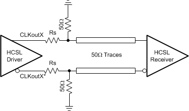
GUID-445C15CC-41CA-440D-8174-69782E87CE00-low.gifFigure 9-6 HCSL Operation, DC Coupling