JAJSGV2D January   2012  – September 2021 LMK01801

PRODUCTION DATA  

  1. 特長
  2. アプリケーション
  3. 概要
  4. Revision History
  5. Device Comparison
    1. 5.1 Functional Configurations
  6. Pin Configuration and Functions
  7. Specifications
    1. 7.1 Absolute Maximum Ratings
    2. 7.2 Recommended Operating Conditions
    3. 7.3 Thermal Information
    4. 7.4 Electrical Characteristics
    5. 7.5 Serial MICROWIRE Timing Diagram
    6. 7.6 Typical Characteristics
  8. Parameter Measurement Information
    1. 8.1 Differential Voltage Measurement Terminology
  9. Detailed Description
    1. 9.1 Overview
    2. 9.2 Functional Block Diagram
    3. 9.3 Feature Description
      1. 9.3.1  High-Speed Clock Inputs (CLKin0/CLKin0* and CLKin1/CLKin1*)
      2. 9.3.2  Clock Distribution
      3. 9.3.3  Small Divider (1 to 8)
      4. 9.3.4  Large Divider (1 to 1045)
      5. 9.3.5  CLKout Analog Delay
      6. 9.3.6  CLKout0 to CLKout11 Digital Delay
      7. 9.3.7  CLKout12 and CLKout13 Digital Delay
      8. 9.3.8  Programmable Outputs
      9. 9.3.9  Clock Output Synchronization
      10. 9.3.10 Default Clock Outputs
    4. 9.4 Device Functional Modes
      1. 9.4.1 Programmable Mode
      2. 9.4.2 Pin Control Mode
      3. 9.4.3 Inputs / Outputs
        1. 9.4.3.1 CLKin0 and CLKin1
      4. 9.4.4 Input and Output Dividers
      5. 9.4.5 Fixed Digital Delay
        1. 9.4.5.1 Fixed Digital Delay - Example
      6. 9.4.6 Clock Output Synchronization (SYNC)
        1. 9.4.6.1 Dynamically Programming Digital Delay
          1. 9.4.6.1.1 Relative Dynamic Digital Delay
          2. 9.4.6.1.2 Relative Dynamic Digital Delay - Example
    5. 9.5 Programming
      1. 9.5.1 Recommended Programming Sequence
        1. 9.5.1.1 Overview
    6. 9.6 Register Map
      1. 9.6.1 Default Device Register Settings After Power On/Reset
      2. 9.6.2 Register R0
        1. 9.6.2.1 RESET
        2. 9.6.2.2 POWERDOWN
        3. 9.6.2.3 CLKoutX_Y_PD
          1. 9.6.2.3.1 CLKinX_BUF_TYPE
          2. 9.6.2.3.2 CLKinX_DIV
          3. 9.6.2.3.3 CLKinX_MUX
      3. 9.6.3 Register R1 and R2
        1. 9.6.3.1 CLKoutX_TYPE
      4. 9.6.4 Register R3
        1. 9.6.4.1 CLKout12_13_ADLY
        2. 9.6.4.2 CLKout12_13_HS, Digital Delay Half Shift
        3. 9.6.4.3 SYNC1_QUAL
        4. 9.6.4.4 SYNCX_POL_INV
        5. 9.6.4.5 NO_SYNC_CLKoutX_Y
        6. 9.6.4.6 CLKoutX_Y_OFFSET_PD
        7. 9.6.4.7 SYNCX_FAST
        8. 9.6.4.8 SYNCX_AUTO
      5. 9.6.5 Register R4
        1. 9.6.5.1 CLKout12_13_DDLY, Clock Channel Digital Delay
      6. 9.6.6 Register R5
        1. 9.6.6.1 CLKout12_ADLY_SEL[13], CLKout13_ADLY_SEL[14], Select Analog Delay
        2. 9.6.6.2 CLKoutX_Y_DIV Clock Output Divide
      7. 9.6.7 Register 15
        1. 9.6.7.1 uWireLock
  10. 10Application and Implementation
    1. 10.1 Typical Application
      1. 10.1.1 Detailed Design Procedure
        1. 10.1.1.1 Driving CLKin Inputs
          1. 10.1.1.1.1 Driving CLKin Pins With a Differential Source
          2. 10.1.1.1.2 Driving CLKin Pins With a Single-Ended Source
        2. 10.1.1.2 Termination and Use of Clock Output (Drivers)
          1. 10.1.1.2.1 Termination for DC-Coupled Differential Operation
          2. 10.1.1.2.2 Termination for AC-Coupled Differential Operation
          3. 10.1.1.2.3 Termination for Single-Ended Operation
  11. 11Power Supply Recommendations
    1. 11.1 Current Consumption
  12. 12Layout
    1. 12.1 Layout Guidelines
      1. 12.1.1 Pin Connection Recommendations
        1. 12.1.1.1 Vcc Pins and Decoupling
        2. 12.1.1.2 Unused clock outputs
        3. 12.1.1.3 Unused clock inputs
        4. 12.1.1.4 Unused GPIO (CLKoutTYPE_X)
        5. 12.1.1.5 Bias
        6. 12.1.1.6 In MICROWIRE Mode
    2. 12.2 Thermal Management
  13. 13Device and Documentation Support
    1. 13.1 Documentation Support
    2. 13.2 Receiving Notification of Documentation Updates
    3. 13.3 サポート・リソース
    4. 13.4 Trademarks
    5. 13.5 Electrostatic Discharge Caution
    6. 13.6 Glossary
  14. 14Mechanical, Packaging, and Orderable Information

パッケージ・オプション

メカニカル・データ(パッケージ|ピン)
サーマルパッド・メカニカル・データ
発注情報
Driving CLKin Pins With a Differential Source

Both CLKin ports can be driven by differential signals. It is recommended that the input mode be set to bipolar (CLKinX_BUF_TYPE = 0) when using differential reference clocks. The LMK01801 family internally biases the input pins so the differential interface should be AC coupled. The recommended circuits for driving the CLKin pins with either LVDS or LVPECL are shown in Figure 10-1 and Figure 10-2.

GUID-EA13DC14-DF53-4308-815B-B28E2ED6A1CD-low.gifFigure 10-1 CLKinX/X* Termination for an LVDS Reference Clock Source
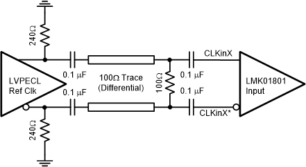
GUID-F58F6C35-FB4F-4DCC-940F-36BFA728D600-low.gifFigure 10-2 CLKinX/X* Termination for an LVPECL Reference Clock Source

Finally, a reference clock source that produces a differential sine wave output can drive the CLKin pins using the circuit shown in Figure 10-3. Note: the signal level must conform to the requirements for the CLKin pins listed in the Section 7.4.

GUID-B3261F25-0B80-4C08-9BEE-D37BCB030B56-low.gifFigure 10-3 CLKinX/X* Single-Ended Termination